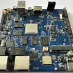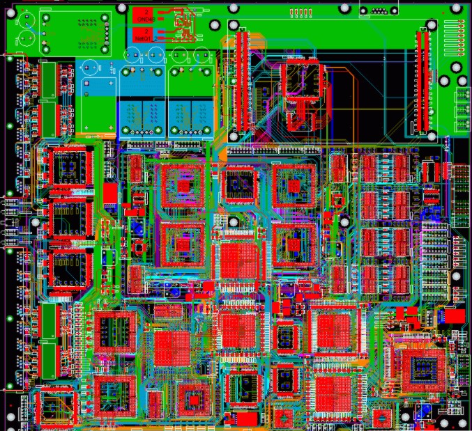
The rapid development of electronic technology continues to create new challenges for board-level design. As electronic systems become faster, smaller, and more highly integrated, PCB designers must deal with increasingly complex electrical and physical constraints.
First, the growing number of high-density pins and the physical limitations of smaller pin sizes make component placement and routing more difficult. Second, increases in system clock frequency introduce new challenges related to timing, signal integrity, electromagnetic interference, and power integrity. Third, engineers increasingly require advanced PC-based design tools to handle complex, high-performance PCB designs efficiently.
These developments have driven several important trends in modern PCB Design:
- High-Speed PCB Design, characterized by higher clock frequencies and faster signal edge rates, has become increasingly common.
- Product miniaturization and higher performance require designers to address distributed electromagnetic effects caused by mixed-signal designs, including digital, analog, and RF circuits on the same PCB.
- Increasing design complexity has made traditional design processes and methods less effective. Modern EDA tools and advanced PCB design platforms are therefore becoming essential for handling high-speed and high-density designs.
As a result, successful PCB Design is no longer limited to connecting components electrically. Designers must consider transmission-line effects, return-current paths, impedance, crosstalk, grounding, power distribution, and EMC throughout the entire design process.
High-Frequency PCB Routing Guidelines
High-frequency circuits require careful routing because signal behavior is strongly affected by trace geometry, component placement, vias, reference planes, and return-current paths. The following principles are important for reliable High-Frequency PCB design.
1. Use Multilayer PCB Structures
High-frequency circuits typically have high integration and high routing density. Using multilayer boards provides sufficient routing space while also helping control electromagnetic interference.
A properly designed multilayer stackup can provide dedicated signal layers, power planes, and ground planes. Continuous reference planes reduce return-path impedance and help maintain controlled impedance for high-speed signals.
For advanced PCB Layout, the layer stackup should therefore be determined early in the design process rather than treated as a manufacturing detail at the end.
2. Minimize Sharp Bends in High-Frequency Traces
The traces connecting high-frequency components should be as straight as practical. When a routing direction must change, designers should use smooth bends, 45-degree routing, or curved transitions rather than abrupt right-angle corners.
The purpose is not simply mechanical reinforcement of the copper. At high frequencies, trace geometry can affect impedance discontinuity and current distribution. Carefully designed bends help reduce unnecessary reflection and electromagnetic coupling.
In high-speed PCB Layout, maintaining consistent trace width and reference-plane conditions is generally more important than following a single universal bend-angle rule.
3. Keep High-Frequency Connections Short
The traces between high-frequency component pins should be as short as possible.
A longer trace introduces additional inductance, capacitance, propagation delay, and opportunities for electromagnetic coupling. At high frequencies, even a relatively short PCB trace can behave as a transmission line.
Therefore, critical components such as clock generators, high-speed transceivers, amplifiers, and RF devices should be positioned close to the components they directly interact with.
Shorter interconnects can improve Signal Integrity and reduce the risk of unwanted radiation and crosstalk.
4. Minimize the Number of Vias
The number of layer transitions in a high-frequency signal path should be minimized whenever possible.
Every via introduces parasitic inductance and capacitance and can create an impedance discontinuity. These effects become increasingly significant as signal rise times become faster.
For critical high-frequency signals, designers should avoid unnecessary vias and carefully evaluate via dimensions, anti-pads, surrounding copper, and return-via placement.
A via should therefore not be considered merely a physical connection between PCB layers. In high-speed applications, it is part of the signal path and must be included in the overall Signal Integrity analysis.
5. Control Parallel Routing and Crosstalk
Closely spaced parallel traces can cause capacitive and inductive coupling. This crosstalk can introduce unwanted noise into sensitive signal lines.
Whenever possible, avoid routing high-speed signal lines in parallel for long distances. If parallel routing cannot be avoided, increase the spacing between traces and consider using a ground trace or grounded copper area as an isolation structure.
For multilayer boards, adjacent signal layers should preferably use routing directions that are perpendicular to each other. This approach reduces broadside coupling between neighboring layers.
A continuous reference plane below or above a high-speed trace can also provide a low-impedance return path and help contain the electromagnetic field.
6. Use Ground Guarding for Sensitive Signals
Ground guarding can be used around particularly sensitive signal lines or critical circuit areas.
Ground traces, copper shielding areas, and strategically positioned ground vias can help reduce electromagnetic coupling. In RF and high-speed designs, ground vias should be placed appropriately to connect the surrounding copper to the reference plane.
However, ground guarding should not be implemented blindly. Poorly designed ground structures can create unwanted current paths or discontinuities. The grounding strategy should always be consistent with the overall stackup and return-current path.
7. Avoid Unnecessary Signal Loops
Signal traces should not form unnecessary loops, and ground connections should be designed to avoid unintended circulating currents.
A well-designed PCB Layout provides a clear current path from the source to the load and an equally clear return path.
For high-speed signals, the return current tends to follow the path of lowest impedance beneath the signal trace. If the reference plane is interrupted, the return current may be forced to take a longer path, increasing loop area and potentially worsening EMI.
8. Place High-Frequency Decoupling Capacitors Close to ICs
Each integrated circuit should have appropriate high-frequency decoupling capacitors located as close as possible to its power pins.
The purpose of a decoupling capacitor is to provide a low-impedance local current source during transient switching and reduce high-frequency power noise.
The effectiveness of a decoupling capacitor depends not only on its capacitance value but also on its package, mounting location, via structure, and connection length.
For this reason, the capacitor should be connected to the IC with the shortest practical path, minimizing parasitic inductance.
9. Manage Analog and Digital Ground Connections
Mixed-signal systems often contain analog, digital, and RF circuits on the same PCB. Improper grounding can allow high-frequency digital noise to enter sensitive analog or RF circuits.
When analog ground and digital ground must be connected, the connection strategy should be determined according to the circuit architecture and current-return requirements.
In some applications, high-frequency filtering components such as ferrite beads or common-mode chokes may be used to control unwanted high-frequency noise. These components should be selected according to the operating frequency, current, impedance, and noise characteristics of the system.
The objective is not simply to separate analog and digital grounds physically, but to control where high-frequency currents flow.
Electromagnetic Compatibility (EMC) in PCB Design
The EMC performance of a PCB is affected by almost every aspect of the design, including PCB material, layer count, component selection, component placement, trace geometry, power distribution, grounding, and interconnection length.
Integrated circuits are important sources of electromagnetic interference. Rapid switching edges can generate broadband noise that propagates through signal traces, power networks, ground structures, and parasitic coupling paths.
Traditional EMI control methods include proper component placement, optimized routing, power distribution, grounding, filtering, and shielding. These techniques remain fundamental to modern PCB Design.
1. Keep High-Speed Signal Traces Short
High-frequency digital signal traces should be kept as short as practical.
The faster the signal edge, the more likely a PCB trace is to exhibit transmission-line behavior. Long traces increase propagation delay and provide greater opportunity for crosstalk and radiation.
Critical clock, reset, memory, and high-speed interface signals should therefore be routed carefully with controlled impedance and a continuous reference plane.
2. Organize Critical Signals Around the PCB Core
Critical signal routing should be carefully organized rather than distributed randomly across the board.
Clock-generation circuits should be positioned close to the devices they drive. Clock distribution should also be designed to minimize unnecessary branching, skew, and coupling.
Depending on the interface and timing requirements, appropriate clock-distribution structures may include point-to-point, daisy-chain, or carefully designed parallel topologies.
3. Keep Power Networks Away from Sensitive High-Speed Signals
Power traces should be separated from sensitive high-speed signal traces whenever practical. Ground copper or a dedicated reference plane can be used to improve isolation.
For multilayer PCBs, placing power and ground planes close together can reduce power-distribution impedance and provide useful high-frequency decoupling.
The power distribution network should be designed with low inductance and low impedance. Wide copper planes, short connections, multiple vias, and appropriately placed decoupling capacitors can all contribute to improved power integrity.
4. Maintain Continuous Reference Planes
One of the most important principles in high-speed PCB Layout is maintaining a continuous reference plane.
A high-speed signal routed across a split or gap in its reference plane may force the return current to travel around the discontinuity. This increases the current-loop area and can significantly increase EMI and signal-integrity problems.
If a high-speed signal must cross a plane transition, an appropriate return-path structure should be provided. Ground stitching vias or carefully positioned capacitors may be used depending on the design architecture.
Designers should avoid unnecessary splits in ground planes, particularly beneath critical high-speed signal paths.
5. Separate Input and Output Routing
Input and output traces should not be routed closely and in parallel for long distances.
When an output signal couples into an input signal, unwanted feedback can occur, potentially causing oscillation, instability, or increased noise.
Where separation is insufficient, a grounded copper region or ground trace can be introduced between sensitive input and output paths.
6. Optimize Trace Width and Spacing
PCB trace width should be selected according to current requirements, impedance requirements, copper thickness, temperature rise, manufacturing capability, and application requirements.
For high-speed signals, trace width and spacing directly affect characteristic impedance and coupling.
For power networks, wider traces or copper planes generally reduce resistance and inductance. For controlled-impedance signals, however, simply making the trace wider is not necessarily better. Trace width must be calculated together with dielectric thickness, dielectric constant, copper thickness, and the surrounding reference-plane structure.
The minimum trace spacing should also meet the PCB manufacturer’s manufacturing capability and the required electrical isolation.
7. Properly Separate Digital, Analog, and RF Areas
Mixed-signal PCB designs require careful partitioning.
Digital circuits, analog circuits, and RF circuits should be arranged according to their noise sensitivity and signal-flow relationships. High-speed digital circuits should be kept away from sensitive analog and RF circuitry whenever possible.
However, physical partitioning alone does not guarantee good EMC performance. Signal routing and return-current paths must also be controlled.
High-speed signals should not cross inappropriate plane boundaries or gaps between different power domains. If a signal must transition between reference regions, the return path should be carefully designed.
8. Control Power and Ground Noise
Power and ground structures are two of the most important contributors to PCB EMI and EMC performance.
High transient currents can generate voltage fluctuations across power-distribution impedance. Similarly, rapidly changing return currents can produce ground noise and electromagnetic radiation.
To minimize these effects, designers should:
- Use low-inductance power and ground structures.
- Place decoupling capacitors close to IC power pins.
- Minimize current-loop areas.
- Use sufficient copper width and plane area.
- Provide multiple ground vias where appropriate.
- Maintain continuous reference planes.
- Keep noisy switching circuits away from sensitive analog or RF circuits.
- Optimize the placement of power regulators and switching devices.
These measures help reduce both conducted and radiated noise.
Practical Considerations for Modern High-Speed PCB Design
As system performance continues to increase, High-Speed PCB Design requires a more comprehensive approach than traditional schematic-to-layout workflows.
Designers should consider electrical behavior from the earliest stages of development. Component placement, layer stackup, impedance requirements, routing topology, power distribution, and grounding strategy should be developed together.
Simulation tools can also be used to evaluate signal integrity, power integrity, electromagnetic coupling, and thermal behavior before prototype fabrication. This helps identify potential problems earlier and reduces the number of PCB design iterations.
For advanced products, design teams should also consider manufacturing capability during the layout stage. Trace width tolerance, via size, registration accuracy, copper thickness, dielectric thickness, and surface finish can all influence the final electrical performance of a PCB.
Kingda’s Approach to High-Speed PCB Manufacturing
For modern high-speed and high-frequency applications, the PCB manufacturer plays an important role in translating the design into a reliable physical product.
Kingda can support high-performance PCB projects by combining manufacturing process control with practical PCB fabrication experience. Key considerations include controlled trace geometry, multilayer stackup requirements, via structures, registration accuracy, copper distribution, impedance control, and manufacturing consistency.
A successful high-speed PCB is not determined by routing rules alone. The design, material selection, stackup, manufacturing process, and electrical requirements must work together.
By considering Signal Integrity, EMI, and EMC requirements from the beginning of the design cycle, engineers can improve system reliability, reduce debugging time, and achieve more predictable high-speed performance.
Conclusion
The continued evolution of electronic technology is driving PCB designs toward higher speed, greater density, smaller form factors, and increasingly complex mixed-signal architectures.
Effective High-Speed PCB Design requires careful control of routing, trace geometry, vias, grounding, power distribution, return-current paths, and electromagnetic coupling. At the same time, High-Frequency PCB designs require greater attention to transmission-line behavior, impedance discontinuities, parasitic effects, and RF signal integrity.
A well-planned PCB Layout should therefore integrate signal integrity, power integrity, and EMC considerations from the beginning. With appropriate design methodologies, simulation tools, and manufacturing controls, engineers can build reliable PCBs capable of meeting the electrical and mechanical requirements of today’s high-performance electronic systems.