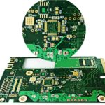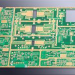
As electronic products continue to evolve toward higher performance, smaller form factors, and greater integration, Power Integrity has become an essential consideration in modern PCB Design.
High-performance processors, FPGAs, memory devices, networking ICs, and other high-pin-count components often operate with multiple power rails and increasingly low supply voltages. As operating voltages decrease, the allowable power-supply noise margin can also become smaller, making the design of a stable power delivery system increasingly challenging.
A well-designed PCB power system must deliver sufficient current with low impedance while minimizing voltage fluctuations, transient noise, electromagnetic interference, and unwanted interactions between power rails.
Modern simulation and analysis tools can help engineers evaluate these problems before prototype fabrication. However, simulation should be considered part of a broader design methodology that includes stackup planning, power distribution, grounding, component placement, decoupling, routing, and manufacturing considerations.
Why Power Integrity Matters in PCB Design
In earlier generations of electronic products, power distribution was often treated as a relatively simple DC design problem. Modern high-speed devices have changed this situation.
A processor can switch large numbers of transistors simultaneously, creating rapid transient current demands. The PCB power delivery network must respond quickly to these changes without allowing excessive voltage fluctuation.
The power system can be affected by:
- Power-plane resistance
- Plane inductance
- Via inductance
- Trace impedance
- Package parasitics
- Capacitor ESR and ESL
- Connector impedance
- Voltage regulator characteristics
- Load transient behavior
- Resonance within the power distribution network
These factors determine how effectively power reaches the IC.
Therefore, Power Integrity should be considered from the earliest stage of PCB Design, rather than being treated as a problem that is solved only after the PCB has been manufactured.
Power Distribution Network (PDN)
A Power Distribution Network (PDN) is the complete electrical path between a voltage regulator and the power pins of an IC.
A typical PDN may include:
- Voltage regulator modules
- DC/DC converters
- Ferrite beads or filters
- Power planes
- Copper traces
- Vias
- PCB capacitors
- Package connections
- IC power pins
The objective of the PDN is to maintain an appropriate voltage at the load under both steady-state and transient operating conditions.
A low-impedance PDN generally provides better control of supply-voltage fluctuations. However, simply reducing impedance everywhere is not enough. Engineers must also consider resonances, anti-resonances, current distribution, thermal requirements, component tolerances, and the frequency range of the load transients.
Multiple Power Rails in Modern Electronics
Modern high-performance ICs commonly require several voltage domains.
For example, a complex system may have separate rails for:
- Core logic
- I/O
- Memory
- Analog circuits
- RF circuits
- PLLs
- High-speed interfaces
- Auxiliary functions
Different voltage rails may have different current requirements and noise tolerances.
Some analog or RF circuits are particularly sensitive to supply noise, while high-current digital processors can generate substantial transient disturbances.
Consequently, power architecture should consider not only the nominal voltage level but also current demand, transient response, noise sensitivity, sequencing requirements, and interaction between different rails.
Power and Ground Plane Design
One of the fundamental tasks in PCB Design is establishing an appropriate power and ground structure.
A multilayer PCB often uses dedicated or partially dedicated plane layers to distribute power and provide low-impedance return paths.
A properly designed Power Plane can provide a broad current-distribution path and reduce resistance compared with narrow traces. A continuous Ground Plane can also provide a low-inductance return path for high-speed signals.
However, splitting power or ground planes should not be performed automatically.
Unnecessary plane splits can force return currents to take longer paths, increasing loop area and potentially causing signal-integrity or EMI problems.
Plane partitioning should therefore be based on actual circuit requirements, current paths, noise sensitivity, and system architecture.
Power Plane Voltage Drop
DC voltage drop is another important consideration in Power Integrity.
When current flows through PCB copper, resistance produces a voltage drop. The approximate relationship is:
V = I × R
As current increases, even relatively small resistance can produce a meaningful voltage difference.
Designers can reduce DC voltage drop through appropriate choices of:
- Copper thickness
- Trace width
- Plane area
- Via quantity
- Via size
- Current distribution
- Power-entry location
For high-current applications, the complete current path from the regulator to the load and back through the return network must be evaluated.
Decoupling Capacitors
Decoupling Capacitors are one of the most important components in a PCB power delivery system.
When an IC suddenly demands additional current, the power supply and PCB cannot always respond instantaneously. A properly selected capacitor placed near the load can temporarily supply part of the transient current and reduce local voltage fluctuation.
However, adding as many capacitors as possible is not necessarily the best solution.
Excessive or poorly selected capacitors can:
- Increase component count
- Consume valuable PCB area
- Increase cost
- Introduce additional parasitics
- Create unwanted resonances
- Complicate assembly
The goal is therefore to determine the appropriate capacitance, quantity, location, and technology based on the actual load and PDN characteristics.
Decoupling Capacitor Placement
The placement of Decoupling Capacitors is often as important as their nominal capacitance.
A capacitor should provide a low-inductance path between the power and ground networks. Excessively long traces or unnecessary vias between the capacitor and IC power pins can increase parasitic inductance.
Important placement considerations include:
- Keep critical decoupling paths short
- Minimize unnecessary vias
- Use suitable via structures
- Place capacitors close to the relevant power pins
- Maintain a low-inductance connection to the reference plane
- Avoid unnecessary routing around the capacitor
- Consider the current path rather than physical distance alone
For complex processors or FPGAs, several capacitor values and package sizes may be used to address different frequency ranges.
Capacitor Selection for Power Integrity
The ideal capacitor does not behave as a perfect capacitor across all frequencies.
Real capacitors have:
- Equivalent series resistance (ESR)
- Equivalent series inductance (ESL)
- Self-resonant frequency
At frequencies above the capacitor’s useful operating range, parasitic inductance can dominate its impedance.
Therefore, capacitor selection should consider the frequency spectrum of the transient current and the complete PDN rather than simply choosing the largest capacitance.
Engineers may evaluate:
- Capacitance
- Voltage rating
- ESR
- ESL
- Self-resonant frequency
- Package size
- DC bias characteristics
- Temperature characteristics
- Tolerance
Simulation and measurement can then be used to verify whether the selected capacitor network provides sufficient performance.
Power Integrity and Signal Integrity
Signal Integrity and Power Integrity are closely related.
Noise on the power distribution network can affect sensitive signal circuits, clock systems, analog blocks, and high-speed interfaces.
At the same time, fast signal transitions can inject noise into the power and ground structures through parasitic coupling.
This interaction is often referred to as simultaneous switching noise or power/ground bounce.
For high-speed systems, engineers should therefore evaluate both signal and power behavior.
Important considerations include:
- Reference-plane continuity
- Return-current paths
- Crosstalk
- PDN impedance
- Ground bounce
- Simultaneous switching
- Power-plane resonance
- Via transitions
- Electromagnetic coupling
A PCB that passes basic DC power checks may still experience high-frequency power-integrity problems.
PDN Impedance and Resonance
The impedance of the PDN varies with frequency.
At low frequencies, voltage regulators and bulk capacitors may dominate the response. At higher frequencies, PCB planes, vias, component packages, and local decoupling capacitors become increasingly important.
The interaction between multiple capacitors and the PCB power structure can create resonant or anti-resonant peaks.
These peaks may increase the impedance of the PDN at specific frequencies and lead to unwanted supply-voltage noise.
Therefore, PDN analysis should examine impedance across the relevant frequency range instead of evaluating only the DC resistance.
Simulation Before PCB Prototyping
Power-integrity simulation can help engineers identify potential problems before manufacturing physical prototypes.
Depending on the tool and model availability, engineers may analyze:
- DC voltage drop
- Current density
- PDN impedance
- Resonance
- Plane behavior
- Decoupling performance
- Transient response
- Power noise
- Thermal effects
Simulation can also support what-if analysis.
For example, designers can compare different capacitor values, placement strategies, power-plane structures, via configurations, or stackups before committing to hardware.
This can reduce the number of prototype iterations and help shorten the overall development cycle.
Power Integrity Analysis of PCB Planes
The power and ground structures can be evaluated before and after layout completion.
Early analysis can help identify potential problems with:
- Power-plane geometry
- Current concentration
- Voltage drop
- Ground return paths
- Via placement
- Plane transitions
- High-current regions
- Sensitive power domains
Post-layout analysis can then use the actual PCB geometry and component placement to provide a more realistic assessment.
This two-stage approach allows engineers to identify architectural problems early and verify detailed implementation later.
Designing for Low Power-Supply Noise
A clean power supply does not depend on a single component or design technique.
It is the result of the complete power delivery system.
Key design practices include:
- Define the power architecture early.
- Identify the voltage and current requirements of every major IC.
- Establish appropriate power and ground structures.
- Minimize unnecessary current-loop area.
- Place decoupling capacitors close to the relevant loads.
- Select capacitors based on impedance and frequency characteristics.
- Control power-plane and via resistance.
- Maintain continuous high-speed signal reference paths.
- Evaluate PDN resonance.
- Validate critical power rails through simulation and measurement.
This systematic approach is generally more effective than adding components after power noise problems have already appeared.
Power Integrity and PCB Stackup
The PCB Stackup has a major influence on power and signal performance.
A well-planned multilayer stackup can provide:
- Low-inductance power distribution
- Continuous ground reference
- Controlled impedance
- Short signal-return paths
- Better electromagnetic performance
- Efficient routing
For high-speed systems, signal layers should be positioned appropriately relative to reference planes. Power and ground structures should also be arranged according to current requirements and signal-return considerations.
The stackup must simultaneously satisfy electrical, mechanical, thermal, and manufacturing requirements.
Manufacturing Considerations
A theoretically optimized power structure still needs to be manufacturable.
Manufacturing tolerances can affect:
- Copper thickness
- Trace width
- Plane geometry
- Via dimensions
- Dielectric thickness
- Layer registration
- Impedance
- Capacitance between planes
Therefore, PCB Design should be coordinated with the manufacturer’s actual process capabilities.
For high-performance products, designers should communicate critical requirements such as controlled impedance, copper thickness, dielectric thickness, via structure, and stackup tolerances before production.
Kingda’s PCB Power Integrity Approach
At Kingda, Power Integrity can be considered as part of the complete PCB development and manufacturing process.
For high-speed and high-density boards, power architecture, multilayer stackup, power and ground planes, via structures, decoupling strategy, and signal routing should be evaluated together.
Kingda can support customers in reviewing PCB structures from a manufacturability perspective and identifying potential issues related to layer configuration, copper distribution, routing density, via structures, and other manufacturing constraints.
Combining appropriate PCB Design practices with controlled PCB Manufacturing processes helps create power delivery systems that are stable, manufacturable, and suitable for demanding electronic applications.
Conclusion
Power Integrity has become an essential part of modern high-performance PCB development.
As supply voltages decrease and IC switching speeds and current demands increase, power distribution networks must deliver stable power with sufficiently low impedance across the relevant operating-frequency range.
Effective power-integrity design requires more than simply adding Decoupling Capacitors. Engineers must consider the complete Power Distribution Network, including regulators, planes, traces, vias, capacitors, component packages, and IC power pins.
A well-designed Power Plane, continuous Ground Plane, optimized capacitor network, appropriate PCB Stackup, and coordinated signal-routing strategy can significantly improve the electrical performance of a high-speed system.
By combining simulation, careful layout, manufacturability analysis, and hardware validation, engineers can identify power-delivery problems earlier, reduce prototype iterations, and develop more reliable electronic products.