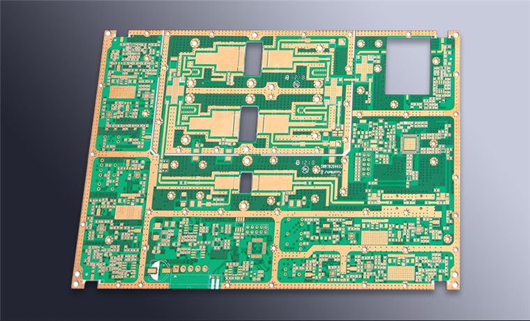
The PCB Manufacturing Process varies according to the board type, layer count, material system, design complexity, and manufacturing technology. Although the basic principles of PCB fabrication have remained relatively stable, advances in imaging, drilling, plating, lamination, surface treatment, and inspection technologies have significantly changed modern production methods.
A simple single-sided PCB may require only a relatively short sequence of processes, while a high-density Multilayer PCB or HDI board can involve numerous additional operations, including sequential lamination, laser drilling, desmear, microvia formation, and advanced registration control.
For this reason, there is no single manufacturing sequence that applies to every PCB. Instead, manufacturers develop a process flow according to the board structure, material requirements, design specifications, and required reliability.
A typical industrial PCB Manufacturing Process can be summarized as:
Engineering and CAM Preparation → Material Preparation → Inner-Layer Fabrication → Lamination → Drilling → Hole Preparation and Plating → Outer-Layer Circuit Formation → Solder Mask → Silkscreen → Surface Finish → Profiling → Electrical Testing → Final Inspection → Packaging and Shipment
The following sections explain the major stages in detail.
1. Engineering and CAM Preparation
Before physical fabrication begins, the manufacturer’s engineering team reviews the customer’s PCB design data.
This stage is an essential part of modern PCB Fabrication because manufacturing problems can often be identified before production materials are processed.
The engineering review normally includes:
- Gerber or other manufacturing data
- Drill files
- PCB stackup information
- Board dimensions and outline
- Copper thickness
- Material specifications
- Surface finish requirements
- Solder mask and silkscreen data
- Controlled impedance requirements
- Electrical test requirements
- Special manufacturing instructions
The CAM team checks clearances, hole sizes, annular rings, line widths, spacing, layer registration, board outlines, and other manufacturing constraints.
Design-for-manufacturing analysis can also identify potential problems such as insufficient copper spacing, inadequate annular rings, extremely small features, or drill-to-copper clearance issues.
This engineering stage is particularly important for complex Multilayer PCB products because the final fabrication process must be compatible with the intended stackup and manufacturing tolerances.
2. Material Selection and Panel Preparation
The next stage of the PCB Manufacturing Process is material preparation.
For conventional rigid PCBs, common materials include FR-4-based laminates, while high-frequency, high-speed, thermal, automotive, and other specialized applications may require different material systems.
Material selection can affect:
- Electrical performance
- Dielectric constant
- Dielectric loss
- Thermal reliability
- Mechanical stability
- Moisture resistance
- Dimensional stability
- Impedance control
- Lamination behavior
The laminate is then cut into production panels according to the manufacturing plan.
Panelization is important because multiple PCB units can often be fabricated on a single production panel. Proper panel utilization improves material efficiency while providing sufficient spacing for tooling, routing, testing, and process handling.
3. Inner-Layer Circuit Fabrication
For a Multilayer PCB, the inner-layer circuits are fabricated before the individual layers are laminated together.
The copper-clad laminate is first cleaned and treated to provide a suitable surface for photoresist adhesion.
A photoresist is then applied to the copper surface. The desired circuit pattern is transferred through imaging technology, such as conventional phototools or laser direct imaging.
The general sequence includes:
- Copper surface cleaning
- Photoresist application
- Circuit imaging
- Exposure
- Development
- Copper etching
- Photoresist stripping
- Optical inspection
During etching, unwanted copper is removed while the copper protected by the resist remains as the circuit pattern.
Modern production may use automated optical inspection (AOI) to identify defects such as open circuits, shorts, line-width abnormalities, missing features, or unwanted copper residues.
The inner-layer process must be tightly controlled because these layers become inaccessible after lamination.
4. Inner-Layer Inspection and Surface Treatment
After inner-layer etching, the copper pattern is inspected to confirm that it meets the design requirements.
AOI is commonly used to compare the fabricated pattern with the original manufacturing data.
Typical inspection items include:
- Trace width
- Trace spacing
- Pad dimensions
- Clearance
- Copper defects
- Open circuits
- Shorts
- Pattern deformation
- Registration accuracy
After inspection, the copper surface may undergo controlled treatment to improve adhesion during subsequent lamination.
Cleanliness is also critical. Dust, oil, oxidation, or other contamination can negatively affect interlayer bonding and may contribute to reliability problems such as delamination.
5. Multilayer PCB Lamination
Lamination is one of the most important stages in Multilayer PCB manufacturing.
The prepared inner layers are assembled together with prepreg and copper foil according to the designed PCB Stackup.
Prepreg is a glass-fiber material impregnated with partially cured resin. During lamination, the resin softens, flows, fills the required spaces, and then cures under controlled temperature and pressure.
A typical lamination sequence includes:
- Inner-layer preparation
- Stackup alignment
- Prepreg placement
- Copper foil placement
- Registration
- Vacuum application
- Heating
- Pressure control
- Resin flow
- Curing
- Controlled cooling
The lamination parameters must be matched to the material manufacturer’s specifications and the required dielectric structure.
Incorrect lamination conditions can cause problems such as:
- Delamination
- Resin voids
- Layer misregistration
- Excessive resin flow
- Board warpage
- Uneven dielectric thickness
- Poor interlayer adhesion
For high-speed designs, lamination also affects dielectric thickness and therefore can influence controlled impedance.
6. Drilling
After lamination, the completed multilayer panel is drilled to create the holes required for component mounting, vias, tooling, and other functions.
CNC mechanical drilling is widely used for conventional through-holes and many via structures.
The drilling process must control:
- Hole diameter
- Hole position
- Drill depth
- Registration
- Drill tool wear
- Hole-wall quality
- Burr formation
For advanced HDI structures, laser drilling may be used to form microvias.
The appropriate drilling method depends on the board structure and design requirements. Mechanical drilling and laser drilling are complementary technologies rather than interchangeable processes.
After drilling, the panel may undergo deburring and cleaning to remove drilling residues.
7. Desmear and Hole Preparation
Drilling through a multilayer board can leave resin smear on the copper surfaces inside the drilled holes.
If this contamination is not properly removed, it can interfere with electrical interconnection between copper layers.
Therefore, drilled panels may undergo a desmear and hole-conditioning process.
The exact chemistry and sequence depend on the laminate material and production technology.
The objectives are to:
- Remove resin residue
- Clean hole walls
- Expose the required copper connection
- Improve adhesion for subsequent metallization
- Prepare the holes for reliable copper deposition
This stage is particularly important for PCB Plating because the quality of the hole wall directly affects plated-through-hole reliability.
8. Electroless Copper and PCB Plating
One of the defining characteristics of a double-sided or multilayer PCB is the ability to electrically connect different copper layers.
After drilling and hole preparation, the hole walls must therefore become conductive.
An electroless copper process can deposit a thin conductive copper layer over the hole walls and exposed copper surfaces. Subsequent electroplating increases the copper thickness to meet the required electrical and mechanical specifications.
This stage is a critical part of PCB Plating.
The process must provide reliable copper coverage throughout the hole wall, especially for plated-through holes.
Important control factors include:
- Copper thickness
- Hole-wall coverage
- Plating uniformity
- Current distribution
- Bath chemistry
- Temperature
- Agitation
- Plating time
- Panel-to-panel consistency
Poor plating control can result in insufficient copper thickness, voids, cracks, or poor interlayer electrical connectivity.
9. Outer-Layer Circuit Formation
Once the board has been drilled and metallized, the outer-layer circuit pattern is formed.
A photoresist is applied to the outer copper surfaces, followed by imaging and development.
Depending on the manufacturing process, copper plating is performed in the areas requiring additional copper thickness. The unwanted copper is subsequently removed during the etching process.
A simplified sequence can include:
Clean → Resist Application → Imaging → Development → Pattern Plating → Resist Stripping → Etching → Inspection
The exact sequence varies between manufacturers and process technologies.
Modern PCB Manufacturing requires close control of line width, spacing, copper thickness, etching compensation, and registration.
This becomes especially important for fine-pitch components, high-density interconnects, controlled-impedance traces, and high-speed circuits.
10. Solder Mask Application
After the outer circuit is completed, a solder mask is applied to protect the copper and prevent unintended solder bridging during assembly.
Solder mask is normally applied to both sides of the PCB where required.
The general process includes:
- Surface cleaning
- Solder mask coating
- Pre-drying or tack drying
- Imaging
- Development
- Inspection
- Final curing
The solder mask is selectively removed from areas that need to remain exposed, such as component pads, test points, and other designated conductive surfaces.
Solder mask registration is important for fine-pitch packages because excessive misalignment can reduce the available solderable area or cause unwanted mask coverage.
The required solder mask thickness and opening dimensions depend on the PCB design, copper topography, material, application method, and manufacturing capability.
11. Silkscreen and Component Identification
Silkscreen, also known as legend printing, is used to provide identification and assembly information on the PCB.
Typical information includes:
- Component reference designators
- Polarity indicators
- Pin-1 markings
- Manufacturer information
- Product identification
- Warning symbols
- Assembly references
Silkscreen should not interfere with solderable pads, test points, or other functional areas.
For automated assembly, clear and accurate component markings can also improve production and inspection efficiency.
12. Surface Finish
After solder mask and silkscreen processing, exposed copper pads generally require an appropriate surface finish.
The surface finish protects exposed copper from oxidation and provides a suitable solderable surface.
Common finishes include:
- HASL
- Lead-Free HASL
- ENIG
- ENEPIG
- Immersion Silver
- Immersion Tin
- OSP
The correct finish depends on the component package, soldering process, storage requirements, electrical performance, reliability expectations, and cost.
For example, fine-pitch packages and BGA applications may benefit from a relatively flat surface finish, while other applications may prioritize cost or specific reliability characteristics.
Therefore, surface finish selection should be considered together with PCB design and assembly requirements rather than treated as a one-size-fits-all decision.
13. PCB Profiling and V-Groove
After the major chemical and surface-treatment processes are completed, the PCB panel is separated into individual boards or prepared for assembly.
Common methods include:
- CNC routing
- V-grooving
- Punching
- Laser cutting for selected applications
The appropriate method depends on the board outline, material, thickness, production volume, and assembly requirements.
V-groove is commonly used when boards have relatively straight edges and are intended to remain in a panel during assembly.
CNC routing provides greater flexibility for irregular board shapes.
The manufacturer should consider the final assembly process when selecting the panelization and depanelization method.
14. Electrical Testing
Electrical testing is a critical quality-control stage in PCB Fabrication.
The purpose is to verify that the finished board does not contain unintended opens or shorts and that the electrical connections correspond to the intended design.
Depending on the product, manufacturers may use:
- Flying-probe testing
- Fixture-based testing
- Netlist testing
- Continuity testing
- Isolation testing
- Specialized functional testing
For high-volume products, dedicated fixtures can provide efficient testing, while flying-probe testing can be advantageous for prototypes or lower-volume production because it requires less dedicated tooling.
Testing requirements should be determined during the engineering stage.
15. Final Quality Inspection
After fabrication and electrical testing, the finished boards undergo final quality inspection.
Typical inspection items include:
- Board dimensions
- Layer registration
- Surface condition
- Solder mask quality
- Silkscreen quality
- Surface finish
- Hole quality
- Copper condition
- Warpage
- Electrical performance
- Cosmetic requirements
Depending on the customer’s specification, additional reliability or physical tests may also be required.
The objective is to ensure that the finished PCB conforms to the approved manufacturing data and applicable quality standards.
16. Packaging and Shipment
After final inspection, qualified PCBs are cleaned, counted, packaged, and prepared for shipment.
Packaging must protect the boards against:
- Moisture
- Dust
- Mechanical damage
- Oxidation
- Contamination
- Electrostatic discharge where applicable
Moisture-sensitive or surface-finish-sensitive products may require additional packaging controls depending on their specifications.
Proper packaging is particularly important for PCBs that will be stored before SMT or other assembly operations.
Single-Sided PCB Manufacturing Process
A typical Single-Sided PCB has conductive circuitry on only one side of the substrate.
Its production process is generally simpler than that of a double-sided or multilayer board.
A typical process flow is:
Material Cutting → Surface Preparation → Circuit Imaging/Printing → Development or Etching → Resist Removal → Drilling → Solder Mask → Silkscreen → Surface Finish → Profiling → Electrical Testing → Final Inspection → Packaging
Depending on the manufacturing technology, some steps may be combined or rearranged.
Single-sided boards are commonly used in relatively simple electronic products where circuit density and interlayer connectivity requirements are limited.
Double-Sided PCB Manufacturing Process
A Double-Sided PCB contains copper circuitry on both sides of the insulating substrate.
When plated-through holes are required, the holes must be metallized to electrically connect the top and bottom copper layers.
A typical process flow is:
Material Preparation → Drilling → Hole Preparation → Electroless Copper → Circuit Formation → Copper Plating → Etching → Solder Mask → Silkscreen → Surface Finish → Profiling → Electrical Testing → Final Inspection → Packaging
The exact sequence may vary depending on whether the manufacturer uses panel plating, pattern plating, or other process configurations.
Compared with single-sided boards, double-sided PCBs require tighter control of drilling, registration, plating, and interconnection reliability.
Multilayer PCB Manufacturing Process
A Multilayer PCB contains three or more conductive layers separated by dielectric materials.
Its production process is significantly more complex because the internal circuits must be created before lamination and subsequently connected through plated holes or advanced via structures.
A typical Multilayer PCB process includes:
CAM Engineering → Material Preparation → Inner-Layer Imaging → Inner-Layer Etching → AOI → Inner-Layer Treatment → Layup → PCB Lamination → Drilling → Desmear → Electroless Copper → Copper Plating → Outer-Layer Imaging → Pattern Plating → Etching → Solder Mask → Silkscreen → Surface Finish → Profiling → Electrical Testing → Final Inspection → Packaging
For advanced HDI products, additional sequential build-up, laser drilling, microvia metallization, and repeated lamination cycles may be required.
Comparison of Single-Sided, Double-Sided and Multilayer PCB Processes
| PCB Type | Main Characteristics | Typical Process Complexity |
|---|---|---|
| Single-Sided PCB | Copper circuit on one side | Low |
| Double-Sided PCB | Copper circuits on both sides with optional plated-through holes | Medium |
| Multilayer PCB | Multiple copper layers connected through vias and plated structures | High |
| HDI PCB | Fine features, microvias, sequential build-up and high-density interconnection | Very High |
The actual process complexity depends not only on the number of layers but also on the material, copper thickness, hole structure, line width, spacing, surface finish, impedance requirements, and reliability requirements.
Key Factors Affecting PCB Manufacturing Quality
A reliable PCB Manufacturing Process depends on the interaction between design, materials, equipment, process chemistry, operator control, inspection, and environmental conditions.
1. Registration Accuracy
As the number of layers increases, registration becomes increasingly important.
Misalignment between layers, drilling, solder mask, and surface features can affect electrical performance and assembly reliability.
2. Etching Control
Etching determines the final geometry of copper traces.
Over-etching can reduce trace width, while insufficient etching can leave unwanted copper between conductors.
For controlled-impedance designs, etching geometry can directly affect the finished trace dimensions and electrical performance.
3. Drilling Quality
Hole diameter, position, aspect ratio, drill wear, burrs, and hole-wall quality must be controlled.
For multilayer boards, drilling accuracy is particularly important because the drilled hole must correctly intersect the intended copper structures.
4. Plating Reliability
Copper plating must provide consistent coverage and adequate thickness.
Poor plating quality can lead to electrical opens, cracks, insufficient current-carrying capability, and long-term reliability problems.
5. Lamination Quality
For a Multilayer PCB, lamination determines whether the individual layers become a mechanically stable and electrically reliable structure.
Resin flow, temperature, pressure, vacuum, heating rate, cooling, and stackup design all need to be properly controlled.
6. Cleanliness
Contamination can affect photoresist adhesion, plating quality, solder mask adhesion, surface finish, and long-term reliability.
Therefore, cleaning and surface preparation are important throughout the entire PCB Manufacturing Process.
PCB Manufacturing Process and Modern Technology
As electronic products become smaller and more integrated, PCB manufacturing is moving toward finer lines, smaller vias, higher layer counts, tighter registration, and more advanced materials.
Modern PCB fabrication increasingly incorporates:
- Laser Direct Imaging
- Automated Optical Inspection
- Laser drilling
- Advanced copper plating
- Sequential lamination
- Microvia technology
- Automated electrical testing
- Advanced surface finishes
- Automated production monitoring
For HDI and high-density applications, conventional manufacturing processes may need to be supplemented with sequential build-up and laser microvia technologies.
The selection of process technology should always be based on the actual PCB design and required reliability rather than simply choosing the most advanced process available.
How Kingda Supports PCB Manufacturing
Kingda provides PCB manufacturing solutions covering different board structures and application requirements.
For each project, the manufacturing process can be evaluated according to:
- PCB type
- Layer count
- Material
- Copper thickness
- Minimum line width and spacing
- Hole structure
- Surface finish
- Impedance requirements
- Production volume
- Reliability requirements
Through engineering review, process control, inspection, and manufacturing capability management, Kingda can help customers convert PCB design data into reliable finished boards.
For complex PCB Fabrication projects, early communication between the designer and manufacturer is especially important. DFM review can help identify potential manufacturing risks before production begins and reduce unnecessary redesign or production loss.
Conclusion
The PCB Manufacturing Process is a combination of mechanical, chemical, optical, thermal, and electrical processes.
Although the basic sequence for a simple board may appear straightforward, modern PCB fabrication requires precise control at every stage, from engineering and material preparation to circuit formation, drilling, lamination, plating, solder mask, surface finishing, testing, and final inspection.
The manufacturing flow also changes according to the board structure. A Single-Sided PCB generally requires fewer interconnection processes, while a Double-Sided PCB introduces through-hole connectivity and plating requirements. A Multilayer PCB requires additional inner-layer fabrication, lamination, drilling, plating, and registration control.
As electronic products continue to become smaller, faster, and more integrated, PCB manufacturers must continuously improve process capability, equipment accuracy, material control, and quality management.
For PCB designers and purchasing teams, understanding the PCB Manufacturing Process is valuable not only for selecting a manufacturer but also for creating designs that are manufacturable, reliable, and cost-effective.