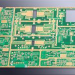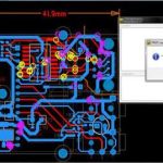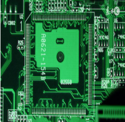
Printed circuit boards are essential components of virtually every electronic product. They provide the electrical and mechanical foundation for connecting and supporting electronic components, making PCB quality directly related to the performance, reliability, and service life of the final product.
During the PCB Manufacturing process, numerous manufacturing variables must be carefully controlled. Material selection, circuit fabrication, lamination, drilling, plating, solder mask application, surface finishing, assembly compatibility, storage, and transportation can all influence the final quality of a PCB.
If these factors are not properly controlled, various PCB Defects may occur. Some defects can be identified through visual or electrical inspection, while others may only become apparent during assembly, thermal cycling, or long-term operation.
Therefore, inspection and reliability verification are essential parts of modern PCB Quality Control.
This article introduces several common PCB quality problems, their potential causes, and practical approaches to prevention and improvement.
1. PCB Delamination
PCB Delamination refers to the separation of layers or interfaces within a PCB, such as separation between copper and dielectric material or between laminated dielectric layers.
Delamination can compromise mechanical integrity and, in severe cases, lead to electrical or reliability failures.
Common Causes
Potential causes include:
- Inappropriate laminate or prepreg selection
- Poor material quality or inconsistent material properties
- Insufficient bonding between layers
- Excessive moisture absorption
- Inadequate lamination parameters
- Contamination on inner-layer copper surfaces
- Excessive thermal stress during soldering or reflow
- Improper packaging or storage
- PCB exposure to high humidity for an extended period
Moisture is particularly important because absorbed moisture can expand rapidly when a PCB is exposed to elevated temperatures during soldering or other thermal processes.
Solutions
To reduce the risk of delamination, manufacturers should establish appropriate material, lamination, storage, and reliability controls.
Recommended practices include:
- Select laminate and prepreg systems appropriate for the application.
- Control material storage temperature and humidity.
- Follow the material supplier’s recommended lamination profile.
- Maintain proper inner-layer surface preparation.
- Control resin flow and bonding conditions.
- Perform thermal stress and reliability testing when required.
- Use appropriate moisture-barrier packaging for finished boards.
- Define shelf-life and handling requirements based on the PCB material and surface finish.
For demanding applications, PCB Reliability Testing may include thermal stress, thermal cycling, humidity exposure, soldering simulation, and other qualification methods.
Tg is also an important material-selection parameter, but a higher Tg alone does not guarantee better reliability. The complete material system, including resin chemistry, CTE, Td, moisture resistance, thermal stability, and processing compatibility, should be evaluated.
Typical Reliability Equipment
Depending on the qualification requirements, manufacturers may use:
- Temperature and humidity chambers
- Thermal shock or thermal cycling chambers
- Soldering simulation equipment
- Thermal stress testing equipment
- Metallographic analysis equipment
2. Poor PCB Solderability
PCB Solderability refers to the ability of exposed PCB surfaces to form reliable solder joints under specified assembly conditions.
Poor solderability can cause insufficient wetting, solder non-wetting, weak joints, solder opens, or other assembly defects.
Common Causes
Possible causes include:
- Excessive storage time
- Improper storage conditions
- Moisture or surface contamination
- Copper oxidation
- Degradation of the surface finish
- Improper surface-finish process control
- Poor solder mask registration
- Solder mask or other residues contaminating solderable pads
- Inadequate handling protection
The selected surface finish also affects solderability and storage performance. Common finishes include HASL, lead-free HASL, ENIG, ENEPIG, OSP, immersion silver, and immersion tin.
Solutions
PCB suppliers should establish clear process-control and acceptance criteria for each surface finish.
For example, when ENIG is used, process monitoring may include:
- Plating bath chemistry
- Gold and nickel process control
- Plating thickness
- Surface condition
- Nickel phosphorus content where applicable
- Bath analysis frequency
- Solderability testing
- Periodic reliability verification
Finished PCBs should also be stored according to the surface-finish supplier’s recommendations.
When boards are stored for an extended period, additional inspection or solderability verification may be appropriate before assembly.
3. PCB Warpage and Bow/Twist
PCB Warpage is a common dimensional problem in PCB manufacturing.
PCB deformation is generally described as bow and twist. Excessive deformation can create problems during SMT assembly, component placement, reflow soldering, connector insertion, and automated handling.
Common Causes
Potential causes include:
- Uneven copper distribution
- Asymmetric PCB stackup
- Improper laminate selection
- Inconsistent lamination conditions
- Excessive thermal stress
- Uneven resin distribution
- Improper cooling after lamination
- Rework or repeated thermal exposure
- Inappropriate storage conditions
- Insufficient process control
Multilayer boards with significantly different copper areas between layers are more susceptible to dimensional stress because copper and dielectric materials have different thermal and mechanical behavior.
Solutions
Manufacturers can reduce warpage risk through:
- Symmetrical stackup design where practical
- Balanced copper distribution
- Appropriate laminate and prepreg selection
- Controlled lamination and cooling
- Proper panel design
- Controlled thermal processing
- Suitable packaging and storage
- Warpage inspection according to applicable specifications
For thin PCBs, flexible PCBs, and large-format boards, additional handling and packaging controls may be necessary.
It is also useful to evaluate PCB warpage under actual assembly conditions rather than relying only on room-temperature measurements.
4. PCB Impedance Variation
Controlled impedance is important for high-speed digital, RF, telecommunications, automotive, and other high-frequency applications.
PCB Impedance Control requires the electrical characteristics of transmission lines to remain within the specified tolerance.
Common Causes
Impedance variation between PCB batches may result from:
- Dielectric thickness variation
- Copper thickness variation
- Trace width variation
- Etching variation
- Dielectric constant variation
- Stackup inconsistency
- Registration variation
- Surface copper roughness
- Manufacturing process variation
Because impedance depends on multiple physical and material parameters, simply controlling trace width is not sufficient.
Solutions
The PCB manufacturer should establish a controlled-impedance manufacturing process that includes:
- Controlled PCB stackup
- Material specification
- Dielectric thickness control
- Trace-width control
- Copper-thickness control
- Etching compensation
- Impedance coupons
- TDR or equivalent impedance testing where applicable
For controlled-impedance products, customers may request impedance test reports for production lots.
The test coupon should represent the actual manufacturing stackup and critical transmission-line geometry as closely as practical.
This allows the manufacturer to verify whether the finished PCB meets the specified impedance requirements.
5. Solder Mask Blistering, Peeling or Poor Adhesion
Solder mask protects PCB copper from environmental exposure and helps prevent unintended solder bridging during assembly.
However, solder mask-related PCB Defects can occur during manufacturing or subsequent thermal processing.
Common problems include:
- Solder mask blistering
- Peeling
- Poor adhesion
- Pinholes
- Misregistration
- Incomplete curing
- Contamination under the solder mask
- Solder mask encroachment onto pads
Common Causes
Possible causes include:
- Improper solder mask material selection
- Inadequate surface cleaning
- Copper surface contamination
- Incorrect pre-curing conditions
- Improper exposure
- Inadequate development
- Incorrect final curing
- Excessive thermal stress
- Rework or repeated heating
- Incompatible assembly conditions
Solutions
A reliable solder mask process should include appropriate control of:
- Copper surface preparation
- Solder mask material
- Coating thickness
- Pre-drying conditions
- Exposure energy
- Development
- Final curing
- Registration
- Thermal resistance
The solder mask system should also be evaluated under the actual assembly process, including reflow, wave soldering, selective soldering, or other thermal processes used by the customer.
6. Black Pad and ENIG-Related Surface-Finish Problems
One common concern associated with ENIG is the phenomenon often referred to as “black pad.”
Black pad is generally associated with problems in the electroless nickel layer and can involve excessive corrosion or abnormal nickel surface conditions during the immersion gold process.
It should not simply be described as a generic “gold and copper potential difference” problem.
Potential Causes
Factors that may contribute to ENIG-related defects include:
- Improper nickel plating conditions
- Excessive corrosion during immersion gold
- Incorrect bath chemistry
- Insufficient process monitoring
- Excessive immersion-gold reaction
- Inappropriate phosphorus content or nickel-layer characteristics
- Poor process stability
Solutions
A reliable ENIG process requires strict monitoring of the chemical process and finished surface.
Important controls may include:
- Nickel bath chemistry
- Gold bath chemistry
- Plating time
- Temperature
- pH where applicable
- Nickel thickness
- Gold thickness
- Surface morphology
- Phosphorus content
- Periodic solderability testing
- Cross-section analysis
- Reliability verification
The exact control limits should be established according to the selected chemistry, process specification, PCB design, and applicable quality requirements.
7. Other Common PCB Defects
In addition to the problems discussed above, PCB manufacturers may encounter many other defects during production.
Open Circuits
An open circuit occurs when an intended electrical connection is interrupted.
Potential causes include:
- Over-etching
- Insufficient copper
- Plating defects
- Scratches
- Broken traces
- Poor drilling or via connection
AOI and electrical testing can help identify these defects before shipment.
Short Circuits
A short circuit occurs when two conductors that should be electrically isolated become unintentionally connected.
Common causes include:
- Under-etching
- Copper residues
- Imaging defects
- Plating abnormalities
- Insufficient spacing
- Contamination
Fine-line PCBs require particularly careful control of imaging and etching.
Hole and Via Defects
Hole-related defects may include:
- Incorrect hole diameter
- Hole position deviation
- Burrs
- Poor hole-wall quality
- Plating voids
- Insufficient copper thickness
- Cracks
These problems can directly affect interlayer connectivity and PCB reliability.
Solder Mask Misregistration
Solder mask openings that are incorrectly positioned can partially cover pads or expose unwanted copper.
This is especially important for fine-pitch components, BGA packages, and other high-density applications.
Surface-Finish Defects
Surface-finish problems can include:
- Uneven coating
- Oxidation
- Poor solderability
- Insufficient thickness
- Excessive thickness
- Contamination
- Surface discoloration
The appropriate inspection method depends on the selected finish.
8. Importance of PCB Quality Control
Effective PCB Quality Control should not depend solely on final inspection.
Quality needs to be controlled throughout the manufacturing process.
A comprehensive quality system may include:
Incoming Material Inspection → Process Control → In-Process Inspection → AOI → Dimensional Inspection → Plating Control → Surface-Finish Inspection → Electrical Testing → Reliability Testing → Final Inspection
Different PCB products require different inspection plans.
For example, a standard single-sided board may not require the same level of testing as a high-layer-count automotive PCB or high-speed server PCB.
The inspection plan should therefore be based on:
- Product application
- PCB structure
- Customer requirements
- Reliability level
- Manufacturing complexity
- Volume
- Applicable industry standards
9. PCB Reliability Testing
PCB Reliability Testing helps evaluate whether a PCB can withstand the environmental, mechanical, thermal, and electrical stresses expected during its service life.
Depending on the application, testing may include:
- Thermal stress testing
- Thermal cycling
- Thermal shock
- Humidity testing
- Solderability testing
- Peel strength testing
- Plated-through-hole reliability testing
- Microsection analysis
- Dimensional stability testing
- Electrical insulation testing
High-reliability applications such as automotive, industrial, medical, aerospace, and telecommunications products may require more extensive qualification.
Reliability testing should be designed according to the product requirements and relevant industry standards rather than applying one universal test program to every PCB.
10. Proper PCB Storage and Handling
Storage conditions can significantly influence PCB quality.
Even a properly manufactured PCB can develop reliability or solderability problems if it is stored incorrectly.
Recommended practices include:
- Maintain appropriate temperature and humidity
- Use moisture-resistant packaging when required
- Avoid unnecessary exposure to ambient air
- Protect finished surfaces from contamination
- Avoid excessive mechanical pressure
- Follow the manufacturer’s shelf-life recommendations
- Use appropriate FIFO inventory management
- Reassess solderability when storage periods exceed specified limits
For moisture-sensitive applications, baking or other moisture-removal procedures should only be performed according to the PCB material, surface finish, and manufacturer’s recommendations.
Excessive or inappropriate baking can also damage certain surface finishes or materials, so baking should not be treated as a universal solution.
11. How Kingda Helps Control PCB Quality
Kingda recognizes that PCB quality is determined by the entire manufacturing system rather than by a single production step.
A reliable manufacturing program should integrate:
- Engineering review
- Material control
- Process control
- Lamination management
- Drilling control
- Plating control
- Circuit inspection
- Solder mask inspection
- Surface-finish control
- Electrical testing
- Reliability verification
- Final quality inspection
For complex PCB projects, early communication between the customer and manufacturer can significantly reduce manufacturing risks.
Kingda can evaluate PCB requirements such as layer count, material, copper thickness, minimum line width and spacing, via structure, controlled impedance, surface finish, and reliability requirements before production.
This approach helps align PCB design requirements with actual manufacturing capability.
Conclusion
PCB defects can originate from material selection, design, manufacturing processes, environmental conditions, storage, or assembly-related thermal stress.
Common problems include PCB Delamination, poor PCB Solderability, PCB Warpage, impedance variation, solder mask defects, plating problems, and surface-finish abnormalities.
The most effective approach is not simply to inspect finished boards and reject defective products. Instead, manufacturers should establish preventive process controls that identify and eliminate potential problems at an early stage.
A comprehensive PCB Quality Control system should combine engineering review, material management, process monitoring, automated inspection, electrical testing, and appropriate PCB Reliability Testing.
By controlling every critical stage from raw material preparation through final inspection, Kingda helps customers obtain PCBs with consistent electrical performance, dimensional stability, solderability, and long-term reliability.