In PCB Design, safety clearance is one of the fundamental considerations for electrical performance, manufacturing reliability, and mechanical compatibility.
Designers need to consider many different types of spacing, including the distance between traces, pads and vias, copper and the board edge, silkscreen and pads, components and neighboring structures, and components and the product enclosure.
These clearances are not simply arbitrary numbers. The appropriate value depends on factors such as operating voltage, signal characteristics, PCB material, manufacturing capability, copper thickness, surface finish, assembly process, environmental conditions, and applicable design standards.
For practical purposes, PCB clearances can be divided into two major categories:
- Electrical clearance
- Non-electrical or mechanical clearance
Understanding the difference between these two categories helps designers create reliable and manufacturable circuit boards.
A. Electrical Safety Clearance
Electrical clearance is primarily related to preventing unintended electrical conduction, arcing, insulation breakdown, and signal interference.
1. Trace-to-Trace Spacing
Trace Spacing refers to the distance between two conductive features, such as copper traces, pads, or other exposed conductors.
The required spacing should be determined according to the electrical requirements and the PCB manufacturer’s process capability.
For low-voltage digital circuits, relatively small spacing may be acceptable when supported by the manufacturer’s manufacturing capability. However, higher-voltage applications generally require larger clearance distances.
Factors affecting trace spacing include:
- Operating voltage
- Transient voltage
- PCB material
- Pollution level
- Environmental humidity
- Conformal coating requirements
- Creepage requirements
- Manufacturing capability
- Applicable safety standards
For many conventional PCB designs, designers may use a practical minimum spacing such as 4 mil or greater when the manufacturer’s process capability allows it. However, this should not be treated as a universal rule.
For fine-line or HDI boards, smaller spacing may be achievable, but the designer should confirm the actual capability with the PCB manufacturer before finalizing the design.
2. Via and Pad Dimensions
Via dimensions include the finished hole diameter, pad diameter, annular ring, and surrounding clearance.
The appropriate via structure depends on whether the design uses:
- Through vias
- Blind vias
- Buried vias
- Microvias
- Mechanical drilling
- Laser drilling
Mechanical and laser drilling have different process capabilities, and the minimum achievable hole size depends on the equipment, material, aspect ratio, copper structure, and manufacturing process.
For example, a conventional mechanical via may use a finished hole diameter around 0.15 mm or larger in some production environments, while laser-drilled microvias can be significantly smaller.
However, designers should always use the manufacturer’s current design rules rather than applying a fixed minimum hole size to every PCB.
In addition to hole diameter, the annular ring must provide sufficient manufacturing tolerance.
Insufficient annular ring can increase the risk of breakout, especially when drilling registration tolerances are taken into account.

3. Pad-to-Pad Spacing
Pad Spacing refers to the distance between adjacent solder pads or other conductive pads.
The required spacing depends on:
- Component pitch
- Package type
- Soldering process
- Solder mask capability
- Assembly tolerance
- Surface finish
- PCB manufacturing capability
Fine-pitch packages, QFNs, BGAs, CSPs, and other high-density components require particularly careful pad and solder-mask design.
A smaller pad spacing does not necessarily mean a better design. The designer should balance routing density with solderability, manufacturing yield, and assembly reliability.
For standard PCB production, a practical spacing of several mils may be commonly used, but the final value should be confirmed according to the manufacturer’s capabilities and the component supplier’s land pattern recommendations.
4. Copper-to-Board-Edge Clearance
Copper should generally be kept away from the PCB edge unless the design specifically requires edge copper, edge plating, or another defined structure.
A suitable PCB Clearance from copper to the board edge helps prevent:
- Exposed copper after routing
- Accidental short circuits
- Edge damage
- Copper peeling
- Manufacturing variation
- Mechanical contact with conductive structures
For conventional PCB designs, designers often use a copper-to-edge clearance of approximately 10–20 mil as a practical starting point.
However, the actual value should be determined according to board thickness, routing method, edge-plating requirements, mechanical tolerance, and the PCB manufacturer’s fabrication capability.
For large copper pours, the copper can be intentionally pulled back from the board edge.
This can be implemented by creating a board-edge keepout region or defining a copper-to-edge clearance rule in the PCB CAD system.
5. Creepage and Clearance for Higher-Voltage PCB Designs
For power electronics and high-voltage applications, ordinary trace-spacing rules may not be sufficient.
Designers should distinguish between clearance and creepage.
- Clearance is the shortest distance through air between two conductive parts.
- Creepage is the shortest distance along the surface of an insulating material between two conductive parts.
The required values depend on the working voltage, insulation system, pollution degree, material characteristics, altitude, and applicable safety standard.
Therefore, high-voltage PCB layouts should be designed according to the relevant product safety requirements rather than simply applying standard low-voltage PCB spacing rules.
This is particularly important for:
- AC power supplies
- Industrial power electronics
- EV and automotive power systems
- Battery management systems
- Motor controllers
- High-voltage converters
- Medical equipment
B. Non-Electrical and Mechanical Safety Clearance
Not all PCB clearances are determined by electrical requirements.
Some spacing requirements exist primarily to ensure manufacturing quality, assembly reliability, component identification, and mechanical compatibility.
1. Silkscreen Character Size and Spacing
Silkscreen is used to identify components and provide assembly information.
Common silkscreen elements include:
- Reference designators
- Polarity markings
- Pin-1 indicators
- Connector labels
- Product information
- Warning symbols
If characters are too small or too close together, they may become difficult to print or read.
Typical silkscreen design values may include character heights around 30 mil or more, with stroke widths selected according to the PCB manufacturer’s printing capability.
The exact minimum character size depends on the silkscreen process, ink type, board surface, and manufacturing capability.
For high-density boards, it is better to prioritize readability and avoid placing excessive text in limited areas.
2. Silkscreen-to-Pad Clearance
Silkscreen should generally be kept away from solderable pads.
If silkscreen overlaps a pad, the printed ink can interfere with soldering or component assembly.
Therefore, the PCB layout should maintain adequate spacing between silkscreen graphics and exposed solderable surfaces.
A clearance of approximately 6–8 mil is commonly used as a practical design reference for conventional production, but the actual value depends on the manufacturer’s silkscreen registration capability.
Modern PCB manufacturers may automatically clip or remove silkscreen that overlaps solder pads during CAM processing.
Nevertheless, designers should not rely entirely on automatic clipping because excessive clipping can remove important component markings.
3. Component-to-Component Clearance
Component placement must consider both the horizontal and vertical dimensions of the components.
Two components may have sufficient spacing on the PCB surface but still interfere with each other because of their package height.
Therefore, PCB Layout should consider:
- Component body dimensions
- Component height
- Connector clearance
- Heat sink dimensions
- Shielding structures
- Cable routing
- Assembly equipment
- Screw and mounting-hole locations
- Product enclosure
- Moving mechanical parts
For example, a tall capacitor may interfere with an enclosure even though its footprint is correctly placed.
Similarly, a connector may require additional clearance for cable insertion and removal.
4. PCB-to-Enclosure Clearance
The PCB should be designed together with the product’s mechanical structure.
Important mechanical references include:
- Enclosure walls
- Mounting posts
- Screws
- Brackets
- Heat sinks
- Fans
- Displays
- Batteries
- Cables
- Connectors
- Shields
The board outline should therefore be checked against the complete mechanical model whenever possible.
Three-dimensional mechanical verification can identify interference before PCB fabrication and assembly.
5. Mounting-Hole Clearance
Mounting holes require special attention because they are often located near the board edge and mechanical structures.
Designers should consider:
- Screw diameter
- Washer dimensions
- Mounting hardware
- Hole tolerance
- Copper clearance
- Grounding requirements
- Chassis connection
- Mechanical stress
If a mounting hole is electrically isolated, an appropriate copper keepout should be provided around it.
If the mounting hole is intentionally connected to chassis ground, the connection structure should be clearly defined in the design.
C. Factors That Determine PCB Clearance
There is no single clearance value suitable for every PCB.
The appropriate PCB Design Safety Clearance depends on several factors.
1. Electrical Voltage
Higher operating voltage generally requires greater electrical clearance and creepage.
Transient voltage should also be considered rather than using only nominal voltage.
2. Signal Frequency
High-speed and RF circuits may require spacing considerations beyond basic electrical safety.
Adjacent traces can couple electromagnetic energy, causing crosstalk and signal-integrity problems.
Therefore, high-speed PCB designs should consider trace spacing together with:
- Trace width
- Reference plane
- Dielectric thickness
- Routing geometry
- Parallel routing length
- Return current path
3. PCB Material
Material properties influence both electrical insulation and mechanical stability.
For high-voltage designs, the insulating properties and relevant material specifications should be considered together with the applicable safety standard.
For high-speed designs, dielectric constant and loss characteristics also influence transmission-line behavior.
4. Manufacturing Capability
A PCB manufacturer may have different capabilities for:
- Minimum trace width
- Minimum spacing
- Minimum hole diameter
- Annular ring
- Solder mask registration
- Silkscreen registration
- Copper thickness
- Layer registration
Therefore, PCB designers should obtain the manufacturer’s latest design-for-manufacturing guidelines before finalizing a high-density design.
5. Assembly Process
PCB clearance should also consider the intended assembly process.
SMT, through-hole assembly, wave soldering, selective soldering, and other processes may have different requirements.
The component land pattern should normally follow the component manufacturer’s recommendations, while solder mask and silkscreen clearances should be verified against the PCB manufacturer’s capabilities.
6. Environmental Conditions
Humidity, contamination, temperature, altitude, and other environmental conditions can affect electrical insulation requirements.
High-reliability applications may therefore require more conservative spacing than ordinary consumer electronics.
D. PCB Clearance and Design for Manufacturing
Good clearance design should be integrated into the complete PCB Design Guidelines rather than added at the end of the layout process.
Before releasing PCB manufacturing data, designers should verify:
- Trace-to-trace spacing
- Trace-to-pad spacing
- Pad-to-pad spacing
- Via-to-pad clearance
- Via-to-trace clearance
- Copper-to-edge clearance
- Silkscreen-to-pad clearance
- Component-to-component clearance
- Component-to-enclosure clearance
- Mounting-hole clearance
- High-voltage creepage and clearance
- Board-to-board mechanical clearance
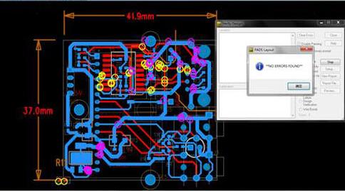
Using CAD design rules can automatically identify many clearance violations before manufacturing.
A DRC check should be performed after routing and again before releasing the final manufacturing files.
E. Practical PCB Clearance Guidelines
The following table can be used as a general design reference. These values are examples rather than universal manufacturing standards.
| Design Item | Typical Reference | Key Consideration |
|---|---|---|
| Trace-to-trace spacing | ≥4 mil for some conventional designs | Voltage and manufacturer capability |
| Fine-line spacing | Manufacturer-specific | HDI and advanced fabrication |
| Mechanical via hole | Often ≥0.15 mm in conventional production | Aspect ratio and drill capability |
| Copper-to-edge clearance | Often 10–20 mil | Board outline and fabrication method |
| Silkscreen character height | Often ≥30 mil | Printing capability and readability |
| Silkscreen-to-pad clearance | Often 6–8 mil | Registration and pad geometry |
| High-voltage clearance | Application-specific | Safety standard and working voltage |
| Creepage | Application-specific | Insulation system and environment |
These values should be treated as PCB Design references rather than fixed industry requirements.
For production boards, the manufacturer’s current capability table and the applicable electrical safety standards should take precedence.
F. How Kingda Supports PCB Design and Manufacturing
A good PCB design should not be separated from manufacturing capability.
Kingda can review PCB designs from the perspective of manufacturability and help customers evaluate critical parameters such as:
- Minimum line width and spacing
- Hole diameter
- Annular ring
- Via structure
- Copper-to-edge clearance
- Solder mask openings
- Silkscreen clearance
- Layer registration
- Controlled impedance
- Board outline
- Surface finish
- Assembly requirements
For high-density or high-reliability PCB projects, early DFM communication can help identify potential problems before production.
Designers can also work with Kingda to determine whether a proposed feature should use a conventional manufacturing process or a more advanced process such as HDI and laser microvia technology.
This approach can improve manufacturing yield while helping maintain the required electrical, mechanical, and reliability performance.
Conclusion
Proper clearance is a fundamental part of reliable PCB Layout and manufacturing.
Electrical clearances help prevent unintended conduction, insulation breakdown, arcing, and signal interference, while mechanical clearances ensure that components, boards, connectors, and product structures can coexist without physical interference.
The most important point is that clearance should not be defined by a single universal number.
Trace spacing, pad spacing, via dimensions, copper-to-edge clearance, silkscreen spacing, and mechanical clearance should all be evaluated according to the PCB design, operating environment, manufacturing capability, assembly process, and applicable standards.
By combining accurate design rules, DRC verification, DFM review, and communication with the PCB manufacturer, designers can reduce manufacturing risks and improve overall product reliability.
Kingda works with customers to align PCB Design Safety Clearance requirements with practical manufacturing capabilities, helping transform complex PCB designs into reliable and manufacturable products.