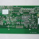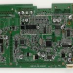
A successful PCB Design project involves much more than drawing a circuit board. It is a systematic process that connects product requirements, hardware architecture, component selection, schematic development, PCB layout, manufacturing, assembly, and testing.
A well-designed PCB should not only meet the required electrical functions but also satisfy mechanical, thermal, reliability, manufacturing, and cost requirements.
From the initial product concept to prototype verification, each stage can influence the performance and manufacturability of the final product. Therefore, engineers should establish clear requirements and consider downstream manufacturing and assembly constraints as early as possible.
This article introduces the major stages of the PCB Design process and explains the key considerations at each stage.
1. Define Product Requirements Clearly
The first step in PCB Design is to define what the product must accomplish.
Before starting the circuit design, engineers should clarify the product’s primary functions, operating environment, mechanical dimensions, interfaces, power requirements, and performance targets.
Important requirements may include:
- Main product functions
- Input and output interfaces
- Supply voltage and power consumption
- Communication protocols
- Sensor requirements
- Processing and storage requirements
- Operating temperature
- Mechanical dimensions
- Enclosure constraints
- User interface
- Reliability requirements
- Regulatory and compliance requirements
- Expected production volume
1.1 Define the Product’s Primary Functions
The main functions should be clearly identified before additional features are introduced.
Optional functions can be added later, but they should not compromise the stability, reliability, cost, or performance of the core functions.
A clear functional definition also helps engineers determine:
- Required ICs
- Number of PCB layers
- Power architecture
- Communication interfaces
- Memory requirements
- Sensor types
- Connector locations
- Approximate board size
1.2 Consider Mechanical Requirements Early
The physical shape of the product can significantly affect the PCB.
Engineers should define:
- Board outline
- Mounting-hole locations
- Connector positions
- Component height restrictions
- Keep-out areas
- Heat-sink locations
- Cable routing
- Enclosure interfaces
For example, a connector that must align with an external enclosure cannot simply be moved after the PCB layout is completed.
Therefore, mechanical and electrical requirements should be developed together during the early planning stage.
2. PCB Hardware System Design
After product requirements have been established, the next step is PCB Hardware Design.
At this stage, the complete hardware architecture is divided into functional blocks.
A typical system may contain:
- Power supply
- Main processor or controller
- Sensors
- Memory
- Communication interfaces
- Analog circuits
- Digital circuits
- RF circuits
- User-interface circuits
- Protection circuits
- External connectors
A system block diagram can be created to show the relationships between these functional modules.
The diagram should clearly illustrate signal flow and power relationships between major blocks.
2.1 Develop a Functional Architecture
A good hardware architecture helps engineers determine how different circuit blocks interact.
For example:
Power Supply → MCU → Sensor → Data Processing → Communication Interface
The actual structure depends on the product.
This approach makes it easier to identify critical signals, power requirements, potential noise sources, and interface dependencies before detailed circuit design begins.
2.2 Plan Power Architecture
Power design should be considered early because almost every circuit block depends on a stable power source.
Engineers should determine:
- Input voltage
- Required output voltages
- Maximum current
- Power-conversion topology
- Voltage regulation
- Power sequencing
- Protection
- Decoupling
- Grounding
- Thermal requirements
For high-performance systems, power integrity can directly influence signal integrity and overall product stability.
3. Component and Device Selection
Component selection is an important stage of PCB Hardware Design.
Typical component categories include:
- Microcontrollers
- Processors
- Power-management ICs
- Sensors
- Memory devices
- Communication ICs
- Transceivers
- Connectors
- Resistors
- Capacitors
- Inductors
- Protection devices
Component selection should not be based only on price.
Engineers should evaluate:
- Electrical specifications
- Package type
- Operating temperature
- Power consumption
- Availability
- Lifecycle status
- Supply-chain stability
- Manufacturer support
- PCB footprint
- Assembly requirements
- Reliability
- Cost
3.1 Evaluate Component Availability
A component that meets all technical requirements may still be unsuitable if it is difficult to procure consistently.
For products intended for mass production, engineers should consider component lifecycle and supply-chain risks during the design stage.
Where possible, alternative components should be identified for critical parts.
3.2 Verify Datasheets and Footprints
Before using a component in a PCB Schematic, engineers should carefully verify:
- Pin definitions
- Electrical ratings
- Recommended application circuit
- Package dimensions
- Land pattern
- Thermal-pad requirements
- Recommended PCB layout
- Power sequencing
- Decoupling requirements
The PCB footprint should correspond to the actual component package and the manufacturer’s recommended land pattern.
An incorrect footprint can cause assembly problems even when the schematic itself is electrically correct.
4. PCB Schematic Design
The schematic represents the electrical relationships within the product.
At this stage, engineers connect components logically before implementing the physical board.
A complete PCB Schematic should clearly define:
- Component references
- Net connections
- Power rails
- Ground connections
- Interfaces
- Protection circuits
- Test points
- Critical signal paths
Good schematic organization makes later PCB layout and debugging significantly easier.
4.1 Divide the Schematic into Functional Blocks
Large designs should be divided into logical sections.
For example:
- Power supply
- MCU
- Analog front end
- Communication
- Memory
- Sensor interface
- RF section
This makes the design easier to review and reduces the possibility of missing connections.
4.2 Add Design Notes and Test Points
Critical circuits should include appropriate test points where practical.
Test points can help engineers measure:
- Supply voltages
- Clock signals
- Communication signals
- Reset signals
- Analog outputs
- Key control signals
Good test-point planning can significantly reduce debugging time during prototype testing.
5. PCB Layout and Routing
After the schematic has been reviewed and validated, engineers can begin the PCB Layout.
The layout converts the logical circuit into a physical PCB structure.
This stage includes:
- Component placement
- Board outline
- Layer stackup
- Routing
- Power distribution
- Ground planes
- Copper pours
- Thermal structures
- Mechanical clearances
- Design-rule checking
5.1 Component Placement
Placement should be based on signal flow, thermal requirements, mechanical constraints, and electromagnetic compatibility.
A typical placement strategy is:
- Define the board outline.
- Place mounting holes and mechanical components.
- Place connectors.
- Place major processors and ICs.
- Place power-management components.
- Place sensitive analog or RF components.
- Place decoupling capacitors.
- Place remaining passive components.
Critical components should be positioned to minimize unnecessary routing distance and unwanted coupling.
5.2 Critical Signal Routing
High-speed and sensitive signals should normally be routed before non-critical signals.
Engineers should consider:
- Trace length
- Trace width
- Differential-pair geometry
- Impedance
- Reference-plane continuity
- Crosstalk
- Via transitions
- Return-current paths
For controlled-impedance designs, routing geometry must be coordinated with the PCB stackup and material properties.
6. PCB Manufacturing and Prototype Production
Once the PCB Layout is complete, the design must be converted into manufacturing data.
The production package may include:
- Gerber files
- Drill files
- Stackup information
- Fabrication drawings
- Material specifications
- Impedance requirements
- Surface-finish requirements
- Solder-mask requirements
- Assembly drawings
- Pick-and-place data
- Bill of materials
6.1 Review Manufacturing Data
Before releasing the design for PCB Manufacturing, engineers should verify:
- Board dimensions
- Layer count
- Copper thickness
- Minimum trace width
- Minimum spacing
- Finished hole sizes
- Annular rings
- Solder-mask openings
- Silkscreen
- Board-edge clearances
- Impedance requirements
- Special fabrication requirements
A DFM review with the PCB manufacturer can identify potential production problems before fabrication begins.
6.2 Gerber Files and Design Security
Gerber files are widely used to communicate PCB fabrication information.
However, the choice between native CAD files and manufacturing output files should be based on the manufacturer’s workflow, required services, data-security policies, and the level of technical information needed.
For production, engineers should work with a qualified manufacturer that can protect design data and clearly define how customer files are handled.
Kingda can work with standard manufacturing data and provide DFM feedback to help identify fabrication risks before production.
6.3 PCB Prototype
Prototype production is an important step before mass production.
A prototype can help verify:
- Electrical functionality
- Component compatibility
- Mechanical fit
- Thermal behavior
- Signal quality
- Power performance
- Assembly feasibility
- Firmware interaction
Prototype cost and lead time depend on factors such as board complexity, material, layer count, quantity, special processes, and manufacturing requirements.
Therefore, fixed prototype prices or delivery times should not be treated as universal standards.
7. PCB Assembly and Soldering
After the PCB is fabricated, components can be assembled.
Depending on the product and production volume, assembly may use:
- SMT assembly
- Through-hole assembly
- Mixed technology
- Automated placement
- Manual assembly
- Reflow soldering
- Selective soldering
- Wave soldering
7.1 SMT Assembly
For surface-mount components, solder paste is normally applied to the PCB using a stencil.
The general process includes:
- Solder paste printing
- Solder paste inspection
- Component placement
- Reflow soldering
- AOI inspection
- Additional inspection or X-ray inspection when required
Fine-pitch packages and bottom-terminated components require careful stencil and pad design.
7.2 Manual Soldering
Manual soldering may be appropriate for prototypes, rework, repairs, or low-volume production.
Typical tools include:
- Soldering iron
- Hot-air rework station
- Tweezers
- Flux
- Solder wire
- Inspection equipment
However, manual soldering quality can vary significantly with operator skill and process control.
For repeatable production, automated assembly and controlled soldering processes generally provide better consistency.
8. PCB Testing and Debugging
After PCB Assembly, the prototype should undergo systematic testing.
Testing should begin with basic electrical checks before applying full operating conditions.
8.1 Visual Inspection
Check for:
- Missing components
- Incorrect components
- Solder bridges
- Insufficient solder
- Component polarity
- Component orientation
- Damaged components
- PCB contamination
8.2 Electrical Testing
Basic measurements may include:
- Power-rail voltage
- Current consumption
- Ground resistance
- Short-circuit checks
- Clock signals
- Communication interfaces
- Reset signals
For more complex products, additional testing may include:
- ICT
- Functional testing
- Boundary-scan testing
- RF testing
- Signal-integrity measurements
- Thermal testing
8.3 Debugging Procedure
A systematic debugging process is more efficient than changing multiple variables simultaneously.
A practical sequence is:
Power → Clock → Reset → Communication → Peripheral → Full Function
This approach helps engineers isolate problems more efficiently.
9. Common Problems During PCB Development
Several problems frequently occur when PCB projects move from design to prototype.
Problem 1: Incorrect Component Footprint
An incorrect footprint can cause:
- Misalignment
- Soldering defects
- Open connections
- Short circuits
- Mechanical interference
Problem 2: Poor Component Placement
Poor placement can create:
- Long signal paths
- Increased crosstalk
- Difficult thermal management
- EMI problems
- Difficult assembly
Problem 3: Insufficient Decoupling
Incorrect capacitor selection or poor capacitor placement can result in power noise and unstable operation.
Problem 4: Manufacturing Constraints Ignored
A PCB may appear correct in CAD software but still be difficult or expensive to manufacture.
Manufacturing capability should therefore be considered before finalizing the design.
Problem 5: Insufficient Prototype Testing
A PCB should not be considered successful simply because it powers on.
Functional, electrical, thermal, mechanical, and reliability-related requirements should be verified according to the product specification.
10. PCB Design Review Before Production
Before releasing a PCB for production, engineers should perform a complete review.
Electrical Review
- Are all nets correctly connected?
- Are power rails correct?
- Are protection circuits included?
- Are critical signals properly routed?
- Are impedance requirements satisfied?
Mechanical Review
- Does the PCB fit the enclosure?
- Are connectors correctly positioned?
- Are mounting holes aligned?
- Are component heights acceptable?
- Are keep-out areas respected?
Manufacturing Review
- Is the design within the manufacturer’s capability?
- Are trace widths and spacings manufacturable?
- Are hole sizes appropriate?
- Is the stackup suitable?
- Are special processes clearly defined?
Assembly Review
- Are component packages suitable?
- Are solder pads correctly designed?
- Is component spacing sufficient?
- Are components accessible for inspection and rework?
- Is panelization appropriate?
11. From PCB Design to Mass Production
Prototype success is only one stage of product development.
Before moving into mass production, the design may need additional optimization based on prototype results.
This can include:
- Component substitution
- Layout optimization
- Thermal improvements
- EMI improvements
- Manufacturing-cost reduction
- Assembly optimization
- Test-point optimization
- Production-panel optimization
The transition from prototype to mass production should therefore involve both engineering validation and manufacturing review.
12. Kingda’s PCB Design and Manufacturing Support
A reliable PCB project requires close coordination between design requirements and manufacturing capabilities.
Kingda can support customers throughout the PCB development process, including PCB Manufacturing, prototype production, and PCB Assembly.
Key areas include:
- DFM review
- PCB fabrication
- Multilayer PCB production
- High-density PCB manufacturing
- Controlled-impedance requirements
- Surface finishing
- SMT assembly
- Through-hole assembly
- Electrical testing
- Manufacturing quality control
By considering manufacturing requirements early in the design stage, engineers can reduce unnecessary redesigns, improve production yield, and achieve a smoother transition from prototype to volume production.
Conclusion
A complete PCB Design process begins with clearly defined product requirements and continues through hardware architecture, component selection, PCB Schematic, PCB Layout, PCB Manufacturing, PCB Assembly, and PCB Testing.
Each stage affects the next. A good schematic supports efficient layout; a good layout improves manufacturing and assembly; and a well-planned prototype provides valuable feedback for final product optimization.
The most reliable approach is to consider electrical performance, mechanical constraints, thermal management, manufacturability, assembly, testing, and supply-chain requirements from the beginning.
By combining sound engineering practices with professional manufacturing support from Kingda, companies can develop PCB products that are easier to manufacture, easier to test, and more reliable in real-world applications.