Wireless Charging PCBA: SMT Assembly Process and Quality Control
Why Wireless Charging PCBA Is Different
Wireless charging has moved quickly from flagship phones into earbuds, wearables, car docks, medical instruments, kitchen appliances and industrial robots. Every one of those products contains the same electronic core: a compact printed circuit board assembly that receives the magnetic field, converts it into clean DC power and manages the charging conversation with the transmitter. Because the board sits millimeters away from a powerful coil, its design and manufacturing rules are stricter than those of an ordinary power supply board.
The receiving side usually combines a resonant tank, a rectifier stage, a charging control IC and a communication decoder on one board. High charging current flows through wide copper traces, while sensitive analog signals share the same laminate. Producing this board well means controlling the full SMT PCB assembly chain: design review, solder paste printing, component placement, reflow soldering and electrical test. This article walks through each stage and explains what determines whether a wireless charger works reliably for years or fails after a few weeks.
Circuit Design and Prototyping Stage
A wireless charging PCBA starts with the electrical design. The engineer selects the coil topology, the resonant capacitor values and the power stage components, then lays out the board so that high current paths are short and the thermal path under the power IC is solid. Copper weight, via stitching and component placement all affect how much heat the board can move away from the coil area, and simulation of the coil field helps avoid interference with nearby metal parts.
Prototyping is equally important. A small batch of sample boards built with the real components reveals pad geometry problems, solder mask issues and reflow behavior before volume production begins. During this stage the PCB design and layout is reviewed against the assembly process, which prevents expensive corrections after thousands of boards have been ordered. Designers should share Gerber files, a complete BOM and assembly notes so the factory can flag risks such as unbalanced copper, oversized thermal pads or components with conflicting reflow requirements.
Solder Paste Printing and Inspection
Once the design is approved, manufacturing begins with solder paste printing. A stencil transfers paste onto the board pads, and the quality of that print controls most of the defects that appear later. Paste that is too thin causes open joints, paste that is too thick causes solder balls and bridging, and paste that is misaligned shifts the whole component. Wireless charging boards are particularly sensitive because power components such as MOSFETs and rectifier diodes depend on large, well filled solder joints to move heat into the copper planes.
Modern lines place a solder paste inspection system right after the printer. SPI measures the height, area and volume of every deposit in seconds and rejects boards outside the process window before any component is placed. This single step eliminates the majority of hidden soldering defects and keeps the reflow oven from becoming a repair station.
Precision Component Placement
After printing, the placement machine picks components from feeders and puts each one on its pad with high accuracy. Wireless charger boards contain a wide mix of parts, from tiny 0201 resistors and capacitors up to QFN power ICs, crystal oscillators and the connectors that carry power to the battery. Modern machines handle the entire range in one pass, using vision systems to correct rotation and position before every placement.
Moisture sensitive devices need attention at this stage. ICs stored without dry packaging absorb humidity, and the trapped moisture can crack the package during reflow. A disciplined factory bakes components that exceed their floor life, logs the exposure time and protects the rest in dry cabinets. Placement data should also be recorded per board so that traceability extends from the reel of components to the finished product in the field.
Reflow Soldering of Wireless Charging Boards
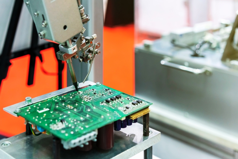
The placed board then enters the reflow oven, where a carefully controlled temperature curve melts the solder and forms the joints. The profile must suit the solder paste, the component mix and the board construction at the same time. Large copper areas near the coil absorb heat faster than thin traces, so a uniform soak zone prevents small components from reaching temperature before the heavy areas do. Peak temperature must be high enough for reliable wetting but low enough to protect plastic housings and sensitive ICs.
Wireless charging PCBA designs often use solder paste on both sides of the board. The second pass is the harder one: components on the bottom side can fall off if the oven profile is too aggressive, so engineers either use smaller parts on the second side or secure heavy components with adhesive. Nitrogen atmosphere and a controlled cooling slope reduce oxidation, improve joint appearance and lower the risk of voids under power pads, which is important for thermal performance.
Inspection and Functional Testing
After reflow, every board should pass automated optical inspection, which checks solder joints, component presence, polarity and alignment at high speed. Boards with hidden solder connections under coil pads or power devices may need X-ray inspection to confirm that the joints are solid and void free. The last gate is electrical test, where each board is powered and its functions are verified rather than only its solder joints.
For a wireless charger, functional test should include the full power path. The board is placed on a reference transmitter, charging current is measured at several output voltages, coil communication is checked and foreign object detection is triggered to confirm the system shuts down safely. These tests, combined with automated optical inspection and process data, are exactly what a mature PCBA testing program delivers before boards are packed for shipment.

Materials, Thermal and Reliability Considerations
Reliability in wireless charging comes from materials as much as from process control. Boards that sit close to the coil must tolerate repeated heating cycles, so the laminate should have a high glass transition temperature and the solder should be a proven lead free alloy. Power components should be derated for the real operating temperature, and the assembly house should verify that solder joints near the coil keep enough strength margin over the product lifetime.
Product safety adds another layer. Because the device charges batteries and communicates over a magnetic field, the design must pass electromagnetic compatibility tests and, where required, wireless charging certification such as Qi. The PCBA manufacturer supports this work by keeping repeatable processes, stable component sourcing and complete documentation, including solder profiles and test records for every batch.
Why Work with a Specialist Factory
Building a wireless charging PCBA in-house means investing in printers, placement machines, reflow ovens, inspection equipment and the engineers who run them. For most product companies, a better route is a contract manufacturer that already owns the line and spreads the investment across many customers. A turnkey PCB assembly service also handles component procurement, which matters for wireless charging boards because coil assemblies and power ICs can have long lead times.
gopcb builds wireless charging boards on modern SMT lines with SPI, AOI and functional test under one roof. Our engineers review the coil layout and thermal design before production, print and profile every batch with recorded parameters, and test the finished assemblies at real charging currents before shipment.
If you are developing a wireless charger, a charging pad or any product that charges through the air, send gopcb your design files and BOM. We will run the DFM review, assemble the PCB assembly in prototype or volume quantities, and deliver boards that charge reliably every time.