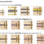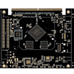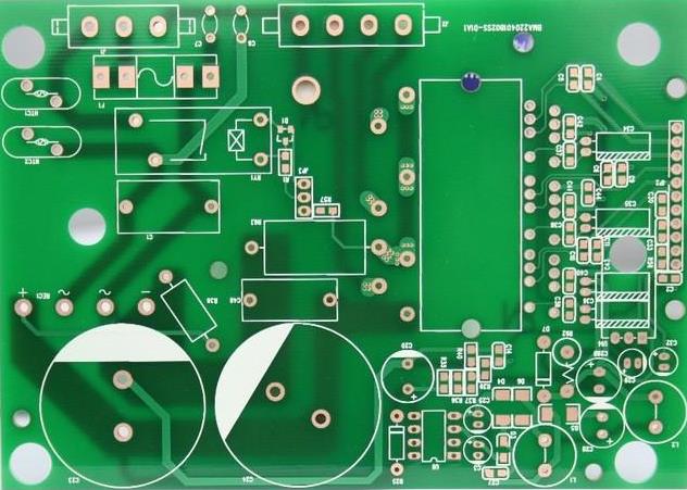
With the rapid development of electronic technology, microwave PCB, high-frequency PCB, and HDI PCB technologies are increasingly used in advanced electronic systems. Their applications now extend across communications, aerospace and defense, scientific research, industrial automation, automotive electronics, medical equipment, and consumer electronics.
As operating frequencies continue to increase and electronic products become smaller and more highly integrated, PCB requirements for signal transmission, dimensional accuracy, material stability, and manufacturing reliability are becoming increasingly demanding.
Compared with conventional FR-4 materials, materials used for high-frequency PCB applications have significantly different compositions and electrical properties. Their glass-fiber structures, resin systems, ceramic fillers, dielectric constants (Dk), and dissipation factors (Df) must be carefully controlled to meet high-frequency signal transmission requirements.
The manufacturing of high-frequency microwave materials for multilayer HDI PCB applications is also more challenging than conventional PCB production. Differences in material hardness, resin content, thermal expansion, copper adhesion, and drilling characteristics can introduce manufacturing problems such as voids, delamination, poor copper bonding, and drilling defects.
This article discusses the key manufacturing technologies for multilayer microwave high-frequency ceramic HDI PCBs, focusing on process optimization, lamination, laser drilling, via filling, and material-specific manufacturing challenges.
1. Definition of Microwave and High-Frequency Technology
The term microwave PCB refers to a circuit board designed to operate at microwave or other high-frequency ranges. Microwave technology generally deals with electromagnetic waves having relatively short wavelengths and high frequencies.
In engineering applications, microwave frequencies commonly range from approximately 300 MHz to 300 GHz, although different industries may use different frequency classifications. At these frequencies, PCB material properties have a much greater influence on electrical performance than they do in conventional low-frequency circuits.
Important material parameters include:
- Dielectric constant (Dk)
- Dissipation factor (Df)
- Dielectric thickness
- Copper surface roughness
- Thermal expansion coefficient
- Moisture absorption
- Dimensional stability
For a high-frequency PCB, even small variations in these parameters can affect impedance, insertion loss, signal attenuation, phase characteristics, and overall signal integrity.
Therefore, material selection and manufacturing process control are essential for high-frequency microwave applications.
2. Material Characteristics of Microwave High-Frequency HDI PCBs
The materials used in a high-frequency PCB are substantially different from standard FR-4 in many applications.
Conventional FR-4 relies primarily on glass fiber and epoxy resin systems. In contrast, microwave and ceramic-based PCB materials may incorporate ceramic fillers or specialized resin systems to achieve controlled dielectric properties and low signal loss.
These materials provide excellent electrical performance but can introduce manufacturing difficulties.
2.1 Low Resin Content
Some ceramic-based prepregs contain very little resin. In certain structures, the resin content can be significantly lower than that of conventional FR-4 prepregs.
This creates several challenges during lamination:
- Reduced resin flow
- Higher risk of interfacial voids
- Lower copper-to-dielectric adhesion
- Greater difficulty achieving uniform bonding
- Increased sensitivity to lamination pressure and temperature
Consequently, the lamination parameters for a ceramic PCB cannot simply be copied from a standard FR-4 process.
2.2 High Material Hardness
Ceramic-filled dielectric materials are often harder and more brittle than conventional PCB materials.
This characteristic affects mechanical drilling, laser drilling, desmear, hole-wall preparation, and copper plating.
Traditional chemical desmear processes may not provide sufficient removal efficiency for certain ceramic-filled materials. Plasma treatment and optimized drilling parameters can therefore become important process options.
2.3 Copper Adhesion
Because of the different surface characteristics and low resin content of some microwave materials, copper adhesion can be weaker than that of conventional FR-4.
The manufacturing process must therefore carefully control:
- Surface treatment
- Lamination pressure
- Temperature profile
- Copper surface condition
- Plating pretreatment
- Hole-wall activation
These controls are particularly important for reliable HDI PCB manufacturing.
3. Original Multistage HDI Manufacturing Process
The original production structure consisted of two core layers, one prepreg layer, and copper foil, followed by multiple lamination cycles.
The blind vias were designed as stacked structures, requiring via filling between successive lamination stages.
The process could be divided into three major lamination stages.
3.1 First Lamination – L3 to L6
The first stage was used to fabricate the inner structure and resin-plugged vias.
The general process included:
Material preparation → Inner-layer imaging → Inner-layer etching → Inner-layer AOI → Brown oxide treatment → Lamination of L3/L6 → Inner-layer imaging → AOI → Surface treatment
The main objective was to establish a stable inner-layer structure before subsequent HDI buildup.
3.2 Second Lamination – L2 to L7
The second lamination stage formed the L2–L7 structure and introduced blind vias associated with the outer buildup layers.
The process included:
Lamination → Brown oxide treatment → Laser drilling → Microsection analysis → Surface treatment → Electroless copper → Full-board copper plating → Microsection analysis → Inner-layer imaging → Etching → AOI → Brown oxide treatment
Laser drilling accuracy and hole-wall quality were particularly important at this stage.
3.3 Third Lamination – L1 to L8
The third stage completed the eight-layer structure and created blind vias on the L1 and L8 sides.
The process generally included:
Lamination → Brown oxide treatment → Laser drilling → Microsection analysis → Copper deposition → Full-board plating → Microsection analysis → Copper reduction → Mechanical drilling → Electroless copper → Full-board plating → Outer-layer imaging → Pattern plating → Outer-layer AOI → Final production
Although this process could produce the required structure, the number of process stages increased manufacturing complexity, cycle time, and cost.
4. Optimized HDI PCB Manufacturing Process
To simplify manufacturing, the original multilayer buildup process can be redesigned by optimizing the core structure and combining certain processing stages.
The optimized process reduces repeated lamination operations while maintaining the required electrical and mechanical structure.
4.1 First Lamination – L3 to L6
The first lamination stage establishes the inner core structure.
A typical process is:
Material cutting → Inner-layer imaging → Copper etching → Inner-layer AOI → Brown oxide treatment → L3/L6 lamination → Inner-layer imaging → AOI → Surface treatment
For blind-via structures, copper pads corresponding to the laser-drilled openings should be designed and processed according to the required laser aperture.
The copper window diameter must be carefully controlled to ensure sufficient alignment tolerance and reliable laser drilling.
4.2 Second Lamination – L1 to L8
The optimized second stage completes the L1–L8 multilayer structure.
A representative process is:
Lamination → Laser-drilling alignment-hole preparation → Blind-via window imaging → Blind-via window etching → Laser drilling → Microsection analysis → Electroless copper → Full-board copper plating → Microsection analysis → Outer-layer pattern preparation → Selective plating and via filling → Microsection analysis → Film stripping → Surface grinding → Mechanical drilling → Electroless copper → Full-board copper plating → Outer-layer imaging → Pattern plating → Outer-layer AOI → Final production
This approach reduces the number of repeated lamination cycles and can improve production efficiency.
At the same time, via filling and laser drilling must be carefully coordinated to ensure that subsequent HDI structures remain aligned.
5. Key Manufacturing Challenges for High-Frequency Ceramic PCBs
The production of a ceramic PCB involves several process challenges that are less significant in conventional FR-4 manufacturing.
5.1 Lamination Void Control
High-frequency ceramic prepregs may have lower resin flow and different bonding behavior compared with conventional FR-4.
Improper lamination conditions can result in:
- Internal voids
- Delamination
- Poor copper bonding
- Uneven dielectric thickness
- Interlayer separation
Therefore, lamination pressure, temperature ramp rate, dwell time, vacuum conditions, and stack-up design must be optimized specifically for the selected material system.
5.2 Copper Foil Adhesion
The low resin content of some high-frequency materials can reduce copper adhesion.
To improve bonding reliability, the manufacturing process should optimize the lamination stack, copper surface treatment, pressure distribution, and thermal profile.
The goal is to achieve sufficient interfacial bonding without damaging the dielectric material.
5.3 Desmear and Hole-Wall Treatment
Ceramic-filled materials can be difficult to process using conventional chemical desmear methods.
For some materials, plasma treatment can improve resin removal and hole-wall preparation.
The process should be optimized together with laser and mechanical drilling parameters to achieve:
- Clean hole walls
- Stable hole diameters
- Low drilling damage
- Reliable copper deposition
- Consistent interlayer connections
This is particularly important when manufacturing fine-pitch HDI PCB structures.
6. Laser Drilling Technology
Laser drilling is one of the most important processes in modern HDI manufacturing.
For blind vias, laser parameters must be optimized according to:
- Dielectric thickness
- Material composition
- Copper thickness
- Laser wavelength
- Pulse energy
- Pulse width
- Beam diameter
- Repetition rate
- Required hole diameter
Improper parameters can lead to resin residue, copper damage, excessive ablation, tapered holes, or insufficient target exposure.
For laser drilling, process engineers must therefore balance drilling efficiency with hole quality.
Microsection analysis should be used to verify:
- Hole diameter
- Hole depth
- Target capture
- Resin removal
- Copper thickness
- Hole-wall condition
- Alignment accuracy
7. Blind Via Filling and HDI Reliability
Blind vias are critical elements in multilayer HDI PCB structures.
When stacked or sequentially built blind vias are used, reliable via filling becomes especially important. Incomplete filling can create cavities, reduce mechanical strength, and affect subsequent lamination or plating processes.
Copper via filling can provide a flat surface for subsequent buildup layers and can also support via-in-pad and fine-pitch component applications.
The filling process must achieve consistent:
- Filling depth
- Copper deposition thickness
- Surface flatness
- Void control
- Electrical continuity
Microsection inspection is an important quality-control method for verifying these parameters.
8. Process Optimization for Cost and Efficiency
The optimized process is not only intended to improve product quality. It can also reduce manufacturing costs.
By reducing unnecessary lamination cycles and integrating certain via-filling and plating processes, manufacturers can potentially reduce:
- Production cycle time
- Material consumption
- Equipment utilization
- Manual operations
- Rework rates
- Manufacturing cost
For PCB manufacturing, process optimization must balance productivity with reliability. A shorter process is not necessarily better if it introduces additional defects.
Therefore, each process change should be validated through engineering trials, microsection analysis, reliability testing, and production verification.
9. Importance of Material-Specific Process Control
One of the most important lessons from microwave and high-frequency ceramic PCB production is that standard FR-4 parameters cannot always be directly transferred to specialized materials.
The manufacturing process should be developed according to the actual material system and board structure.
Key areas requiring customized control include:
- Material storage and conditioning
- Lamination temperature and pressure
- Vacuum control
- Laser drilling parameters
- Desmear or plasma treatment
- Copper deposition
- Via filling
- Mechanical drilling
- Registration accuracy
- AOI and microsection inspection
A controlled process window helps ensure stable electrical performance and mechanical reliability.
10. Kingda’s Approach to Microwave High-Frequency HDI PCB Manufacturing
As advanced electronic systems demand higher frequencies, tighter geometries, and greater integration, manufacturers need strong capabilities in both material engineering and process control.
Kingda can apply a structured manufacturing approach to specialized microwave PCB, high-frequency PCB, and HDI PCB applications, with particular attention to material compatibility, multilayer lamination, laser drilling, via filling, copper plating, and inspection.
For ceramic and high-frequency materials, manufacturing parameters should be developed according to the actual dielectric system rather than simply applying conventional FR-4 process conditions.
Through process optimization and engineering verification, Kingda can help customers address challenges associated with high-frequency multilayer PCB manufacturing while improving production efficiency and consistency.
Conclusion
The development of microwave and high-frequency electronics is driving increasingly demanding requirements for PCB materials and manufacturing processes. Compared with conventional FR-4 boards, ceramic-based high-frequency PCB materials can provide excellent electrical performance but require more specialized manufacturing controls.
The major challenges include low resin content, weak copper adhesion, high material hardness, difficult desmear, laser-drilling sensitivity, lamination voids, and complex blind-via structures.
For advanced HDI PCB manufacturing, process optimization should focus on the complete production chain, from material selection and lamination to laser drilling, via filling, copper plating, AOI, and microsection inspection.
With appropriate material-specific process development and manufacturing control, microwave high-frequency ceramic PCBs can achieve the electrical performance, interconnection density, reliability, and production efficiency required by next-generation electronic applications.