Vias are one of the most important interconnection structures in modern printed circuit boards. They provide electrical connections between different conductive layers and allow signals and power to pass through a multilayer PCB.
As electronic products become smaller and circuit density continues to increase, the correct design and manufacturing of PCB vias have become increasingly important. Different via structures, including through vias, blind vias, and buried vias, are used according to the electrical, mechanical, and routing requirements of the PCB.
For high-density applications, via plugging and advanced drilling technologies are also essential to ensure PCB reliability and manufacturing quality.
Kingda provides professional PCB manufacturing services covering multilayer PCBs, HDI PCBs, high-frequency PCBs, rigid-flex boards, thick copper PCBs, precision double-sided PCBs, and other advanced circuit board technologies.
What Is a PCB Via?
A via is a plated conductive hole used to electrically connect copper patterns located on different layers of a PCB.
In a multilayer PCB, individual copper layers are separated by insulating dielectric materials. These copper layers cannot communicate directly with one another. PCB vias therefore provide the vertical electrical paths required to connect signals and power between different layers.
Unlike component holes, vias are generally not designed to accommodate component leads.
A typical via consists of:
- A drilled or laser-formed hole
- Copper plating on the hole wall
- A copper pad around the hole
- Electrical connections to one or more PCB layers
The via structure and dimensions depend on the PCB stack-up, layer count, signal requirements, current capacity, and manufacturing process.
Types of PCB Vias
The three main types of PCB vias are through vias, blind vias, and buried vias.
Each structure has a different function and manufacturing process.
Through Vias
A through via extends from one outer surface of the PCB through the entire board.
It can connect multiple copper layers along its path and is one of the most commonly used via structures in conventional multilayer PCB manufacturing.
Through vias offer relatively simple manufacturing and good reliability.
However, they occupy routing space on every layer they pass through. As PCB density increases, this can limit available routing channels.
For this reason, high-density PCB designs may use blind vias or buried vias to optimize routing space.
Blind Vias
A blind via connects an outer layer of the PCB to one or more internal layers without passing through the entire board.
Because the via does not extend through the complete PCB, the opposite side of the board cannot be seen through the hole. This is why it is called a blind via.
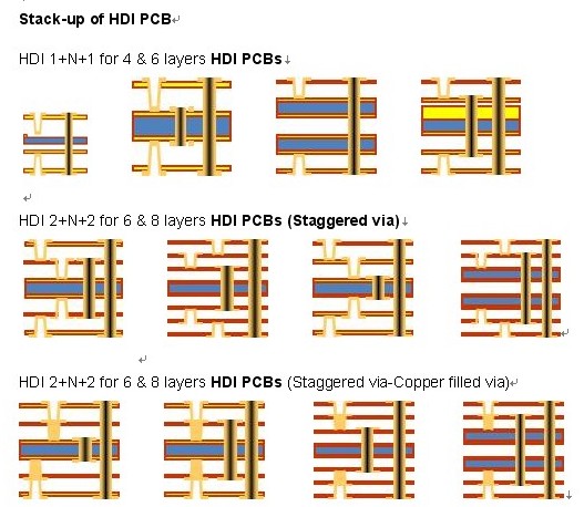
Blind vias are particularly useful in HDI PCB designs because they can increase routing density and provide more efficient use of PCB space.
They are commonly used to connect:
- Top layer to inner layer
- Bottom layer to inner layer
- Surface pads to adjacent internal layers
Blind vias can be manufactured using mechanical drilling or laser drilling, depending on the via diameter, depth, layer structure, and production technology.
Buried Vias
A buried via connects two or more internal PCB layers without extending to either outer surface.
Unlike a through via, a buried via is completely enclosed within the multilayer structure and cannot be directly seen from the outside of the finished PCB.
Buried vias can provide significant routing advantages in high-density designs.
They allow designers to establish interconnections between internal layers without consuming routing space on the outer layers.
However, buried-via manufacturing is more complicated because the relevant inner-layer structures generally need to be fabricated and interconnected before the complete multilayer board is laminated.
As a result, buried vias are typically more expensive than conventional through vias.
Comparison of Via Types
| Via Type | Connection | Manufacturing Complexity | Typical Application |
|---|---|---|---|
| Through via | Outer layer through the entire board | Low to moderate | Conventional multilayer PCBs |
| Blind via | Outer layer to internal layer | Moderate to high | HDI and high-density PCBs |
| Buried via | Internal layer to internal layer | High | High-density multilayer PCBs |
Selecting the appropriate via structure is an important part of PCB stack-up and routing design.
Why Via Plugging Is Used
As PCB technology has developed, via plugging has become increasingly common.
Via plugging refers to filling or sealing a via with a suitable material, often solder mask or resin, depending on the design and manufacturing requirements.
Via plugging may be used to:
- Prevent solder from entering the via
- Reduce solder-ball formation
- Improve surface flatness
- Prevent contamination
- Improve assembly reliability
- Support via-in-pad structures
- Improve thermal and electrical performance in certain designs
The exact plugging method depends on the PCB structure and application.
Requirements for Via Plugging
Different PCB applications may have different requirements for via plugging.
For example, some designs may require the via to be completely filled with copper, while others may use resin filling or solder-mask plugging.
Typical requirements may include:
- Appropriate filling material
- Sufficient filling depth
- Controlled void content
- Reliable adhesion
- Smooth surface finish
- Adequate solder-mask coverage
- No exposed defects around the via
For high-density PCB applications, the via-filling process must be carefully controlled because even small defects can affect assembly reliability.
Via-in-Pad Technology
Via-in-pad technology places a via directly within a component solder pad.
This approach can significantly reduce routing distance and save PCB space.
It is particularly useful for fine-pitch BGA packages and other high-density components.
However, simply placing a conventional open via inside a solder pad can create problems during soldering.
During reflow, solder may flow into the via, resulting in:
- Insufficient solder volume
- Voids
- Solder balls
- Poor joint formation
- Reduced assembly reliability
For this reason, via-in-pad designs commonly require filled and capped vias or other controlled via structures.
PCB Drilling Process
PCB drilling is a critical manufacturing process because vias provide the physical pathways required for interlayer electrical connections.
The basic drilling process creates holes in the copper-clad laminate or multilayer PCB according to the production data.
Depending on the PCB structure, drilling may be performed using:
- Mechanical drilling
- Laser drilling
- UV laser drilling
- CO₂ laser drilling
Mechanical drilling is widely used for conventional through holes, while laser drilling is commonly used for microvias and advanced HDI structures.
Importance of Drilling Accuracy
Drilling accuracy directly affects PCB reliability.
If the hole position deviates from the intended location, it can cause:
- Insufficient annular ring
- Layer-to-layer connection failure
- Open circuits
- Short circuits
- Plating problems
- Reduced manufacturing yield
As PCB line widths and via diameters become smaller, registration accuracy becomes increasingly important.
Manufacturers must therefore carefully control drilling equipment, tooling, panel alignment, and process parameters.
Via Diameter and Board Thickness
The minimum finished hole diameter is closely related to PCB thickness.
One important parameter is the aspect ratio, which represents the relationship between hole depth and finished hole diameter.
As the board becomes thicker and the hole becomes smaller, reliable drilling and copper plating become more difficult.
Therefore, designers should evaluate:
- PCB thickness
- Finished hole diameter
- Drill diameter
- Hole aspect ratio
- Copper plating thickness
- Annular ring
- Drilling tolerance
The actual minimum hole diameter should always be determined according to the PCB manufacturer’s proven process capability rather than relying on a universal value.
Blind Via Manufacturing Challenges
Manufacturing blind vias requires tighter process control than conventional through vias.
When mechanical drilling is used, the drilling depth must be accurately controlled to avoid penetrating unintended layers.
If the hole depth is excessive, it may damage an internal circuit layer or create unwanted electrical connections.
If the hole is too shallow, the intended copper layer may not be properly connected.
Laser drilling can provide more precise depth control for microvia structures, but it also requires careful control of laser energy, dielectric thickness, copper thickness, and process parameters.
Buried Via Manufacturing Challenges
The manufacturing process for buried vias is more complicated.
Because buried vias are located inside the PCB, their interconnection structure must generally be created before the complete multilayer stack is assembled.
A simplified process may include:
- Fabricating the relevant inner layers
- Drilling the buried vias
- Copper plating the via walls
- Inspecting the inner-layer connections
- Laminating additional PCB layers
- Completing drilling and plating operations
- Performing final inspection and testing
This additional processing increases manufacturing time and cost.
However, buried vias can provide valuable routing space in highly integrated PCB designs.
PCB Vias in HDI Manufacturing
HDI PCB technology makes extensive use of small-diameter microvias, blind vias, and sequential build-up structures.
Microvias are generally created using laser drilling and are designed to connect adjacent layers.
Compared with conventional through vias, microvias can significantly improve routing density.
They are particularly useful for:
- Fine-pitch BGA packages
- Smartphones
- Wearable devices
- Compact communication equipment
- Medical electronics
- Automotive electronics
- High-density computing systems
As electronic products continue to shrink, HDI technology is becoming increasingly important for high-density interconnection.
Via Design Considerations
When designing PCB vias, engineers should consider more than simply the hole diameter.
Important design parameters include:
Via diameter: Must be compatible with the selected drilling process.
Pad diameter: Must provide sufficient annular ring and manufacturing tolerance.
Via spacing: Must prevent electrical shorts and provide adequate manufacturing clearance.
Layer connection: The designer must clearly define which layers each via connects.
Current capacity: Vias carrying significant current may require larger diameters, multiple vias, or optimized copper structures.
Thermal performance: Thermal vias may be required to transfer heat from components to internal or external copper planes.
Impedance: High-speed signal vias can introduce discontinuities and should be designed carefully to maintain signal integrity.
Thermal Vias
In addition to electrical interconnections, vias can be used for thermal management.
Thermal vias provide a path for heat to move from a component pad to an internal copper plane or external heat-dissipation structure.
They are commonly used beneath power devices, LEDs, processors, and other components that generate significant heat.
A thermal via array can improve heat transfer, but its design must consider solder flow, via filling, pad structure, and assembly requirements.
PCB Via Reliability
Via reliability is critical because vias experience mechanical and thermal stresses throughout the PCB’s operating life.
During PCB fabrication and assembly, temperature changes can cause different materials to expand and contract at different rates.
Repeated thermal cycling can place stress on the plated copper inside the via.
Reliable via manufacturing therefore requires control of:
- Copper plating thickness
- Hole-wall quality
- Aspect ratio
- Material selection
- Thermal expansion
- Lamination quality
- Drilling quality
- Registration accuracy
For high-reliability applications, manufacturers may also perform thermal cycling, microsection analysis, and other reliability tests.
Choosing the Right Via Structure
The best via structure depends on the PCB’s electrical, mechanical, and manufacturing requirements.
Through vias are suitable when manufacturing simplicity and cost efficiency are priorities.
Blind vias are appropriate when additional routing density is required between surface and internal layers.
Buried vias are useful when internal-layer interconnections must be created without consuming outer-layer routing space.
Microvias are especially suitable for advanced HDI designs and fine-pitch components.
The correct combination can improve routing efficiency while balancing manufacturing complexity and cost.
Kingda PCB Manufacturing Capabilities
Successful via manufacturing depends on both PCB design and production capabilities.
Kingda provides PCB manufacturing solutions for conventional multilayer boards as well as advanced HDI, high-frequency, rigid-flex, and other high-density circuit board applications.
For projects involving blind vias, buried vias, microvias, via-in-pad structures, or other complex interconnections, manufacturers must carefully evaluate drilling, plating, lamination, registration, and inspection requirements before production.
Early communication between PCB designers and manufacturers can help identify potential manufacturing risks and optimize the final design.
Conclusion
PCB vias are fundamental to multilayer circuit board interconnection. Through vias, blind vias, buried vias, and microvias each provide different solutions for connecting conductive layers and optimizing PCB routing.
As PCB designs move toward higher density and smaller dimensions, advanced technologies such as via plugging, via-in-pad, laser drilling, and HDI interconnection are becoming increasingly important.
At the same time, reliable PCB drilling, copper plating, registration control, and inspection are essential to ensure long-term PCB performance.
By selecting the appropriate via structure and working closely with an experienced manufacturer such as Kingda, designers can achieve a better balance among circuit density, electrical performance, manufacturability, reliability, and overall production cost.