



Thermal Management in High-Speed PCB Design
Heat in a fast board comes from more places than the obvious ones. The large devices dominate, but the transmission lines themselves dissipate energy, and at high rates that loss is not negligible. Thermal management is therefore part of the layout rather than a consequence of it: the result is a board whose thermal behaviour is a design property rather than an outcome, and one that has to be arranged while the layout is open: a thermal path added after routing has to compete for the same copper the routing is already using.
Where the Heat Comes From
Four sources contribute, and they scale differently.
Digital devices dissipate power roughly in proportion to the number of gates switching and the square of the supply voltage, which is why core supplies have fallen even as current has risen. Power devices — amplifiers, regulators, switching stages — dissipate energy in the conversion itself. Resistors dissipate wherever current flows through them, and a resistor carrying substantial current in a wide trace is a heat source that is easy to overlook because it is small.
The fourth source is the interconnect. At high frequency the current concentrates near the surface of the conductor, which raises the effective resistance, and the dielectric between the trace and its reference absorbs a fraction of the field on every cycle. Both effects convert signal energy into heat, distributed along the traces rather than concentrated at a component, which makes it invisible to a per-component power budget and significant on a dense, fast board.
Placement as a Thermal Decision
Placement determines how much heat one component receives from another and how easily the assembly can get rid of it.
Heat sources should be spread rather than clustered. Two large devices placed side by side create a local region whose temperature is higher than either would produce alone, and the components surrounding them are then operating outside the conditions the design assumed.
The devices also need to be placed with the enclosure and the airflow in mind. A device positioned where air cannot reach it, or where it sits in the shadow of a taller component, will run hotter than the same device in an open area. Where the design uses a heatsink or a chassis wall as a thermal path, the position of the devices relative to that structure is a placement decision rather than a mechanical detail.
The parts that must stay cool deserve the same attention in the other direction. Electrolytic capacitors lose life rapidly with temperature and are among the first components to fail on a hot board. Crystals drift with temperature, and references change their output. Keeping those components away from the switching devices and out of the warm region around them costs board area and extends the life of the assembly.
<img src="https://www.gopcba.com/wp-content/uploads/2026/04/Solar-Inverter-Systems.jpg" alt="thermal via cluster beneath a high power device” />
The Thermal Path Inside the Board
Heat leaves a component through its own package and then through whatever the board provides. The board’s contribution is copper, and copper used as a thermal structure is a different design from copper used as routing.
The first element is a copper area under the device, larger than the device itself, so that heat spreads into a volume of copper rather than concentrating at the pad. The second is a cluster of thermal vias connecting that area to copper on the other side of the board or to an internal plane. These vias carry no signal, and their design parameters — diameter, plating, count and arrangement — are chosen for heat transfer and manufacturability rather than for electrical reasons.
The third element is the internal plane. A ground or power plane is a large sheet of copper connected to the device through the vias, and it spreads heat laterally across the whole board and radiates it from the entire surface. This is why a board with continuous planes runs cooler than one without, even when nothing else changes.
What defeats the arrangement is an interruption in the path. Copper area under a device connected to the far side through a handful of small vias has a bottleneck, and the bottleneck determines the temperature regardless of how much copper is placed at either end. The path is only as good as its narrowest point.
Materials and Interfaces
Three material choices change the thermal behaviour of an assembly.
Metal-core boards replace the usual laminate beneath the circuit with aluminium or copper, which conducts heat far better than the resin and glass it replaces. They are used where the heat load is high and the space is constrained, and they bring their own design constraints: the metal core is conductive, so the layer adjacent to it must be arranged accordingly, and the machining and plating processes differ from those used on conventional laminates.
Thermal interface materials fill the microscopic gaps between a component and the surface it is mounted to. Air is a poor conductor, and a surface that appears flat has enough roughness to leave an air layer that dominates the path. Grease, a pad or a cured compound removes it, and the choice depends on the mechanical arrangement — a bolted interface can use a thin layer of grease, while a gap that varies with tolerances needs a pad that compresses.
The third is the interface to the environment: the heatsink or the enclosure. A heatsink that is oversized but poorly coupled to the device performs worse than a smaller one that is properly mounted with a controlled interface material and adequate clamping pressure.
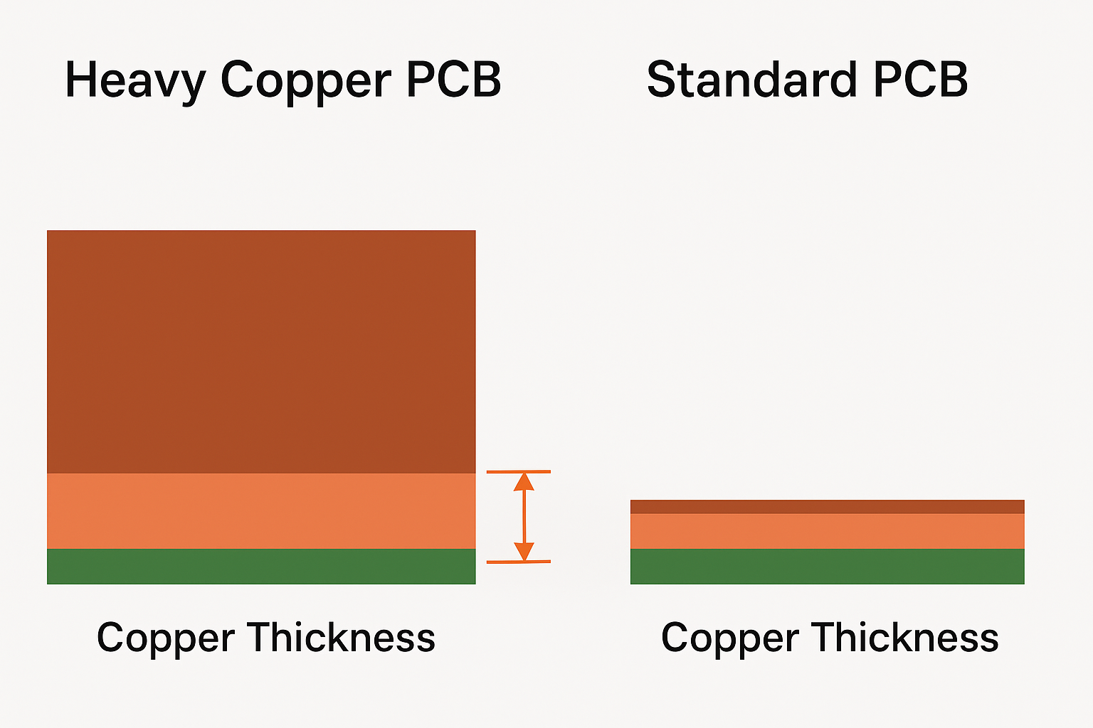
Where a design must carry large currents as well as remove heat, the copper weight itself becomes a design variable, since a thicker conductor both reduces the loss that generates heat and spreads the heat that remains. The trade-offs involved are described in the article on heavy copper in HDI boards.
Routing Choices That Affect Temperature
Three routing decisions have a thermal consequence.
Conductor width determines resistive loss, and where a trace carries substantial current the width should be calculated from the current and an acceptable temperature rise rather than chosen by habit. The second is length: a shorter path has less resistance and less loss, and it also carries less of the dielectric loss that accumulates along a long route. The third is the arrangement of current-carrying paths, which should be direct and free of narrow sections, since a narrow neck in a power path is a local hot spot.
Where the design distributes power through a plane rather than through traces, the plane’s continuity is what determines the losses, and the same continuity provides the thermal spreading described above. The two functions reinforce each other, which is one reason a well-designed supply network also keeps a board cooler.
Structures Beyond the Board
The board is one part of a thermal system that usually continues outside it. Heatsinks increase the surface area available to the air; heat pipes move heat from where it is generated to somewhere it can be removed, using the evaporation and condensation of a working fluid; and vents and ducts in the enclosure determine how much air actually flows across the surfaces that need it.
Forced airflow is the most effective of these, and it is also the one most dependent on layout. A fan that produces a strong flow across an open board is of little use if the components are arranged so that the air passes over them in a thin layer while the larger devices sit in still pockets behind each other. Arranging components so that the airflow reaches the surfaces that generate heat is part of the placement decision.
Measure Rather Than Assume
The last step is verification. A junction temperature calculation for a single device is a starting point; what the assembly does at full load, in its enclosure, at the worst ambient it will see, is what determines whether the design works.
The practical approach is to measure: surface temperatures with contact sensors or a thermal camera on a working board, under the actual load, with the actual airflow. The findings regularly show that the assumption about which component runs hottest is wrong, because the board conducts heat from a large device into a small one that has no path of its own.
The result feeds back into derating: components operated well below their rated maximum temperature last longer, and the ones with the largest temperature sensitivity — electrolytic capacitors and anything with a chemical or resonant element in it — should be given the widest margin in the design.
Where the board carries a power stage, the thermal decisions interact with the layout of the stage itself. The arrangement of devices, current paths and heat spreading in a converter is covered in the article on half-bridge converter layout, and the supply arrangement that feeds the load is described in the guide to power delivery system design.
FAQ
How many thermal vias are enough? Enough that the vias are not the bottleneck in the path. Their combined cross section should be comparable to the copper area they connect to, which usually means a cluster rather than a few holes.
Does a larger heatsink always help? Only when the interface between the device and the heatsink transmits heat efficiently and the heatsink has airflow. A large heatsink poorly coupled to a device performs worse than a smaller one properly mounted.
Why do electrolytic capacitors fail first? Because their life falls steeply with temperature. Placing them away from heat sources is one of the cheapest reliability improvements available at layout time.


3 Comments
High Reliability PCB Design Rules
[…] thermal rules that place components relative to heat sources are covered further in the article on thermal management, the sizing of conductors that carry heavy current in the note on heavy copper, and the acceptance […]
COM Express Carrier Board Layout Guide - Kingda
[…] Thermal design is part of it too. Heat leaves the module through a defined path, and the carrier is normally expected to help conduct it away — through copper, through stiffeners, or into a housing. Treating the carrier as purely electrical tends to produce a design that works on the bench and throttles in the enclosure, which is the same trap described in this note on thermal management on dense boards. […]
Metal Core PCB: Base Materials, Types and Properties - Kingda
[…] The metal is not the only variable. Dissipation also depends on the thickness of the insulating layer and on its thermal conductivity, which is why thermally conductive fillers are added to the dielectric. A thinner insulating layer conducts heat better, but a thinner layer withstands less voltage — so thermal conductivity, voltage withstand and insulation performance have to be weighed together rather than optimised one at a time. That trade-off is the central decision in specifying a metal core board, and it is the same tension that appears in any design where heat must pass through a dielectric, as discussed in this look at thermal management on dense boards. […]