



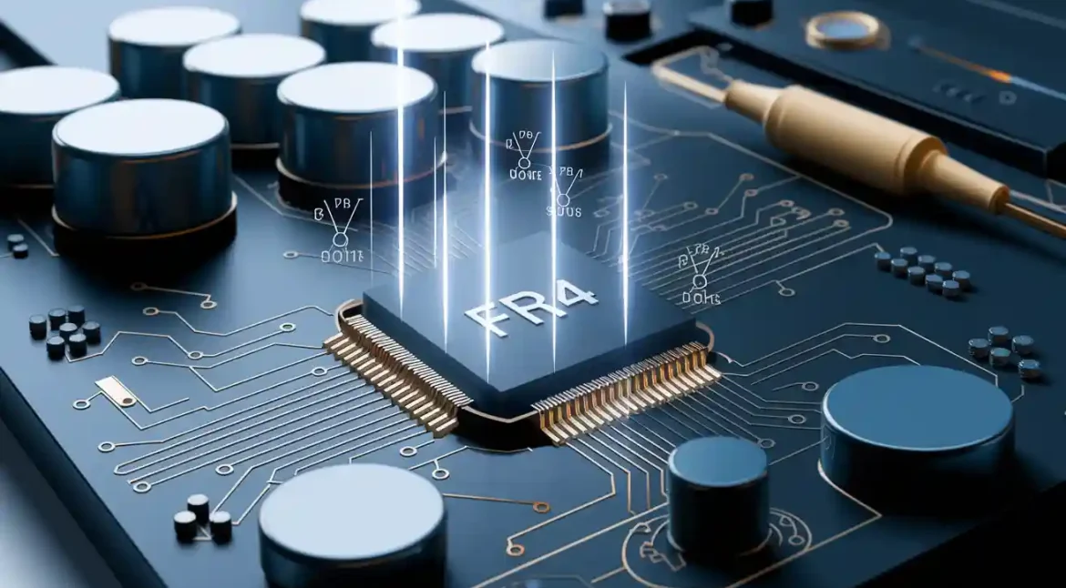
PCB Design Principles for EMI Suppression
Electromagnetic compatibility is not a layer of varnish applied at the end of a project. It is a set of physical decisions taken during layout, and by the time the board is fabricated the opportunity to influence most of them has passed. Two coupling mechanisms dominate: conduction coupling, which is characteristic of low frequencies and travels along conductors, and radiation coupling, which dominates at high frequency and travels through the air. Cutting both paths is the only reliable strategy.
Board Selection and Layer Planning
The first decision that affects EMI suppression is the board itself. Layer count and stackup determine how well a design can control impedance and how much shielding the traces receive. A board whose signal layers sit adjacent to unbroken ground planes has a much lower radiated field than an equivalent design where signals route freely with no reference.
Frequency drives the requirement. As clock rates and edge rates rise, the current loops that a layout creates radiate more efficiently, and the margin available in a two-layer design disappears. Moving to a multilayer board with dedicated planes is often the cheapest available EMC measure, because it converts a widely distributed antenna into a set of tightly coupled transmission lines. It also makes the impedance of every high-speed net predictable, and predictability is what allows a designer to reason about emissions before the board exists. Where a design must pass an EMC test on the first attempt, the stackup decision should be made before the schematic is finished rather than after the layout is complete.
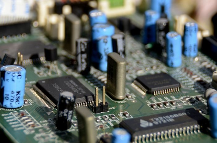
Cutting Conduction Coupling
Conduction coupling travels through shared conductors: a supply rail, a ground network, a signal that carries a switching edge into a neighbouring stage. The countermeasures are local decoupling and separation. Each integrated circuit should have a decoupling capacitor close to its power pins, with a short and wide connection to the ground plane, because the loop formed by the capacitor, the pin and the plane is what determines how effective the capacitor is at high frequency.
Sharing a single capacitor between several devices is a common mistake. The inductance of the trace between the capacitor and the second device dominates the impedance, and the decoupling that the calculation promised never appears. Supply rails that feed several functional blocks should also be separated at the source, either with a ferrite or with an RC filter, so that the noise generated by one block does not reach another through the rail.
Cutting Radiation Coupling
Radiation coupling is controlled by geometry rather than by components. The field strength from a current loop is proportional to the area of that loop and to the square of the frequency, so the practical measures are all about reducing loop area. Routing a signal close to its return plane is the single most effective action available, and it is why the continuous ground plane matters so much.
The return current follows the path of lowest impedance, which at high frequency means directly beneath the trace. If the ground plane is cut, the return detours around the cut, the loop area increases sharply, and the trace radiates. The behaviour of that return current under a divided reference is discussed in more detail in this article on power plane splitting, where the practical widths of the gaps are also given.
Cables attached to the board are the other major radiator. A cable behaves as an antenna driven by whatever common-mode voltage appears at the connector. Keeping the connector ground connection wide and short, tying the connector shield to chassis ground with a low-inductance path, and filtering the signals that leave the board are all effective. The treatment of the board edge itself, where traces can pick up charge, is covered in this discussion of ESD and PCB edge traces.
<img src="https://www.gopcba.com/wp-content/uploads/2026/05/供电柜PCBA.png" alt="clock trace routed away from board edge to reduce radiation coupling” />
Clock and High-Speed Routing Rules
The clock is the most demanding net on the board. Its edges are the fastest in the design, it is periodic, and its harmonic content reaches far into the frequency range where everything radiates. Clock traces should be as short as the placement allows, should never run parallel to a signal that leaves the board, and should be routed away from the board edge and from connector pins. Where a clock must cross the board, route it between ground planes if the stack allows, and keep the trace away from the edge of the plane underneath.
Termination is part of the EMC treatment as much as the signal integrity treatment. A trace whose reflections are not controlled produces ringing, and ringing is simply additional high-frequency energy. Series termination close to the driver is the usual answer for point-to-point nets, while parallel and AC termination have their own roles. The rules on routing angles and escape geometry apply equally here, and are set out in this article on escape routing rules.
Ground Plane Continuity and Via Usage
A ground plane is only effective if it is continuous. Any slot, whether cut deliberately or created accidentally by a dense via field, forces return currents to divert. Vias for signals should be routed with their own accompanying ground via wherever possible, particularly for high-speed nets, so that the return current can change layers alongside the signal. Without that companion via, the return must find a path through the plane capacitance, and the transition becomes a localised discontinuity.
The plane also has to be stitched. Ground copper on different layers should be joined with a regular grid of vias, especially around the perimeter and around connectors. A grid reduces the plane impedance and removes the parallel-plate resonances that can amplify radiated emissions at particular frequencies.
Filters, Shielding and the Last Resort
Filtering is applied to interfaces rather than to the board interior. Common-mode chokes on cable interfaces, feed-through capacitors on connectors and ferrite beads on supply entries all reduce the noise that leaves or enters. These measures are most effective when the ground reference for the filter is a clean chassis connection rather than the digital ground, and they lose most of their value if the return path from the filter is inductive.
Shielding over a whole assembly is the most expensive option and should be considered only after the layout has been optimised. A shield can suppress radiation but it cannot repair poor return path geometry, and it often converts a differential-mode problem into a common-mode problem by adding capacitance to the chassis.
FAQ
What is the difference between conduction coupling and radiation coupling? Conduction coupling travels along conductors and dominates at low frequency, where the wavelength is long compared with the board. Radiation coupling travels through the air and dominates at high frequency, where trace lengths become significant fractions of a wavelength. Most products must deal with both, and the countermeasures are different.
How important is the ground plane to EMI suppression? It is the single most important structural feature. It determines the loop area of every return path, provides the reference for controlled impedance, and acts as the shield between layers. A design with a continuous ground plane will nearly always outperform one without, regardless of the components used.
Can I fix an EMC failure by adding filters at the end of the project? Sometimes, but only partially. Filters address noise that leaves through cables, and they cannot repair radiation from a trace that has a large loop area or from a split plane. Layout geometry sets the floor of the emission spectrum and filtering only trims the peaks above it.


1 Comment
PCB Layout Constraints: Six Checks Before Placement
[…] how close a trace may run to the edge. Board outline and mounting design brings these together, and EMI suppression design principles covers the layout measures that reduce emissions without adding […]