High Speed Routing Questions: Vias, Decoupling and Planes
The same questions come up on almost every high-speed layout, and the answers are more consistent than the variety of the questions suggests. What follows is a set of the recurring ones, with the reasoning behind each answer rather than a rule to be memorised.
What Matters Most When Routing High-Speed Signals
Three things, in order. impedance matching has to be correct, which means the stackup and the trace width have to be chosen together so that the trace presents the impedance the driver expects. The trace has to be isolated from its neighbours, which is a question of spacing and of the plane beneath it. And where the signal is differential, the pair has to be routed as a pair, with matched length and constant spacing.
Differential routing is worth the extra effort on fast digital signals because it makes the receiver’s decision independent of a single-ended threshold. The common-mode noise that the pair picks up cancels at the receiver, which is the property that makes the technique so robust.
Do More Vias Really Hurt the Board
It depends on the signal. For a low-frequency net, a via is a small resistance and a small inductance and it does not matter. For a high-frequency signal, each via is a discontinuity and a stub, and the stub resonates at a frequency determined by its length. That is why the advice on fast nets is to minimise the via count and to use blind or buried vias where the design allows them.
Where the routing simply does not fit, the answer is more layers rather than more vias. Adding a layer costs money once; a stub that resonates costs performance on every board.
Is More Decoupling Always Better
No. A decoupling capacitor helps when it is the right value in the right place, and it does nothing when it is the wrong value or too far from the pin. A large capacitor responds slowly and supplies bulk charge; a small one responds quickly but holds very little. Using only one value leaves a gap in the frequency response, which is why a combination is used.
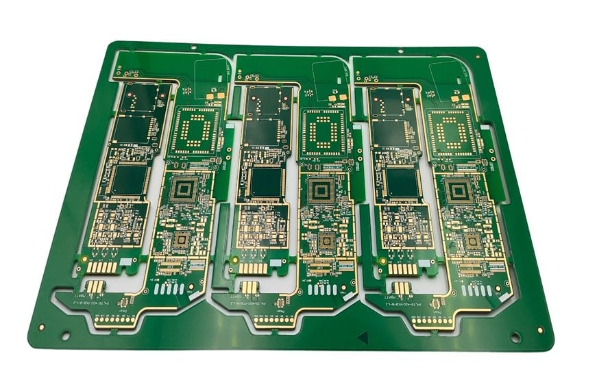
Placement matters more than quantity. A capacitor twenty millimetres from the pin has an inductance that dominates its capacitance at the frequencies where the switching noise actually occurs. Analogue supply pins deserve their own local capacitors, because the supply rejection of an analogue device falls with frequency and cannot be relied on.
What Makes a Good Board
A reasonable checklist is: placement that follows the signal path, power traces with enough copper for the current and some margin, controlled impedance where the signals are fast, and simple, direct routing on the slow nets. Nothing on that list is exotic, and a board that satisfies all four is usually easy to debug.
Through Vias, Blind Vias and Buried Vias
Blind and buried vias increase the density that can be achieved, reduce the layer count needed, reduce the board area and lower the number of plated through holes that pass through every layer. They are the standard tool for high-density interconnect designs.
The trade is cost and process complexity. A through via is drilled after lamination; a blind or buried via has to be formed before the layers are pressed together, which adds process steps and requires tighter registration. That is why most designs use through vias unless the density genuinely requires otherwise. Blind and buried via stack selection covers when the additional cost is justified.
Mixed-Signal Ground Strategy
Where a board has fast analogue signals, the question of whether to split the planes or keep them whole has a practical answer. If the analogue signals are above roughly 20 MHz and there are many of them, give the analogue section two layers: one for the signals and one for a solid ground, with plenty of stitching vias between the signal layer’s ground and the plane.
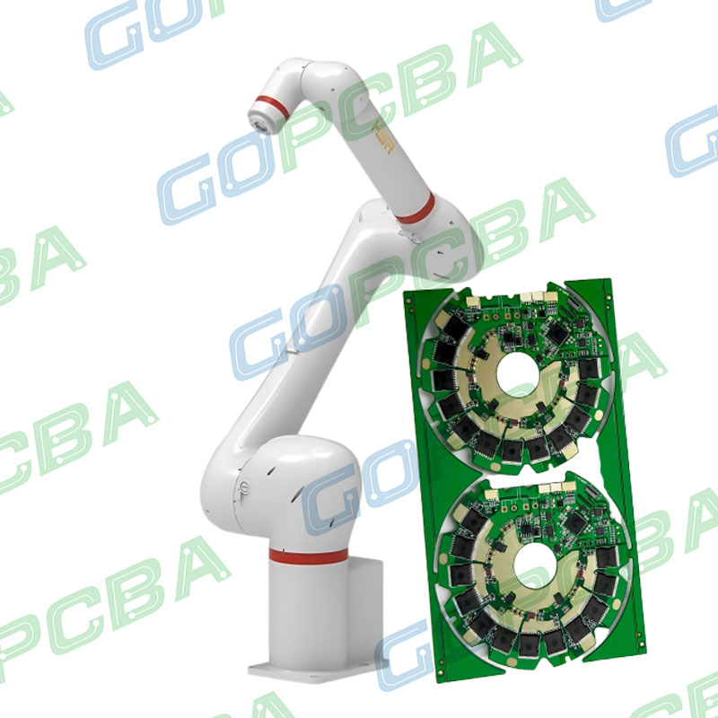
That arrangement gives the analogue signals a controlled transmission medium and a matched impedance, isolates them from the digital section, and keeps the return loop small because the return is a wide plane rather than a trace. Splitting the ground into islands and joining them at one point sounds tidier but forces the return current to detour, which grows the loop. Power plane splitting rules covers the cases where splitting is genuinely required.
Where to Put the Regulator
If the connector and the processor are at opposite ends of the board, the regulator should go close to the load rather than close to the connector. The reason is that the current is highest at the load, and the trace from the regulator to the load carries that current and develops a voltage drop across its resistance. The input side of the regulator carries a higher voltage and a lower current, so a longer path there costs less.
The exception is a design where the regulator’s own dissipation requires it to be near a thermal path or near the board edge, in which case the placement decision is thermal and the trace resistance has to be managed with copper width instead. Trace width and current calculation gives the width needed for both cases.
Blind and Buried Vias in Practice
Where they are used, they should be included in the stackup drawing rather than left implicit in the drill file, because the sequence in which the layers are drilled and pressed determines whether the design can be built at all. A via that passes through three layers but stops inside the board requires a specific lamination order, and the fabricator needs to know that from the start. Via in pad or plated through covers the related decision about where a via may sit.
FAQ
Length Matching and Where It Applies
Length matching is a timing tool, not a general requirement. It matters where several signals are sampled together by a receiver, such as a parallel bus or a group of lanes in a serial link, and it matters within a differential pair at all times. It does not matter on a reset line or a control signal that has no timing relationship with anything else.
Where matching is required, the budget comes from the timing margin of the interface rather than from a habit. A common figure for a parallel bus is a few millimetres of skew between lanes, and intra-pair skew is much tighter, generally under 0.15 mm. Applying a tight tolerance where it is not needed adds routing difficulty and buys nothing.
Serpentine routing is the standard way to add length, and it should be used carefully. Keep the meander pitch loose, keep the gap between adjacent segments at least four times the trace width, and keep the meander away from the ends of the net where reflections accumulate.
Should fast signals be routed on inner layers? Inner layers between planes give a stripline with shielding above and below, which is better for emissions. Outer layers are easier to route and to probe. The usual compromise is to put the most critical nets inside and the rest outside.
How many decoupling capacitors does a design need? One small capacitor per supply pin on a fast device, plus bulk capacitance at the supply entry. Fewer, larger capacitors are cheaper but less effective.
Is it worth using blind vias on a small design? Only if the routing genuinely does not fit with through vias. The cost is in the process, not the material, and it appears on every board in the order.