AIoT Processor Core Board Design Considerations
A modern processor for embedded vision and edge computing packs eight or more cores, a graphics engine, a neural accelerator and a set of high-speed peripherals into a package that may have a thousand balls at a pitch below a millimetre. The core board that carries it is small, dense and unforgiving, and the design decisions that matter are made before any signal is routed.
Layer Planning for a Dense Device
The first decision is the layer count, and it is driven by the escape from the device rather than by the number of nets. A processor with a full ball grid array and multiple memory interfaces typically needs eight to twelve layers, because the inner rows of balls can only be reached through vias that must pass between the balls of the outer rows. Reducing the layer count below that does not simplify the design; it makes the escape impossible.
The layer arrangement matters as much as the count. The memory interface should have its own reference planes, the processor core should sit over a solid ground plane, and the high-speed serial interfaces should be routed on layers that are tightly referenced. Where the board carries both a fast memory bus and an analog or radio section, the partitioning rules described in this discussion of mixed signal design guidelines apply.
Memory Interface Routing
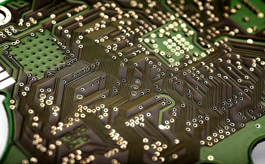
The dual-data-rate memory interface is usually the largest single routing task on the board. Its nets are numerous, its timing margin is small and its routing must be matched within defined groups. The length matching is a delay requirement, not a cosmetic one, and the tolerance is stated in the device documentation as a fraction of a clock period.
The routing discipline follows from that. Each byte lane is treated as a group, with the data lines matched to their strobe and the address and command lines matched within their own group. The reference plane beneath the group must be continuous from the processor to the memory, because a plane change alters the propagation delay of the trace above it and invalidates the matching that was calculated. The techniques that apply to the group as a whole are described in this article on high frequency traces and data buses.
The routing also has to be checked against the plane arrangement, because a reference plane that changes between the processor and the memory invalidates the delay calculation even if the traces are perfectly matched. Keeping the lane on one reference layer from end to end is the simplest way to guarantee that.
`r`n
The memory devices themselves need decoupling at their own supply pins, and the reference voltage for the interface must be quiet. Any noise on the reference appears directly in the sampling threshold and reduces the eye height, which is why the reference is normally generated locally and filtered rather than shared.
<img src="https://www.gopcba.com/wp-content/uploads/2026/08/32-layer-PCB.webp" alt="DDR routing matched in length on an AIoT core board” />
Power Architecture and Sequencing
A device of this class requires several rails with different voltages and different current capabilities, and it usually requires them to come up in a defined order. The core rail may need to be stable before the memory rail is enabled, and the input and output rails may need to rise within a defined time of each other. The design must provide the circuitry that enforces this, and the sequencing must be verified on the first prototype rather than assumed to work.
The power distribution itself is a wideband problem. The regulator handles the low frequency behaviour, the bulk capacitance handles the mid-band, and the capacitors at the pins handle the high frequency. Each level must be placed correctly, because a capacitor that is electrically distant from the pin contributes almost nothing at the frequency where it is needed. The geometry of the distribution network is the same problem discussed in this article on DC-DC converter layout.
Thermal Design
A processor running at multi-gigahertz with several cores active dissipates enough power that the package is designed to shed heat through its base into the board. The board must therefore provide that path: a copper region under the package on the top layer, a dense array of thermal vias, and copper on the inner and bottom layers to spread the heat. The vias must be arranged so that solder does not wick away during reflow, and the thermal pad must reach an adequate solder coverage, because the thermal resistance of the assembled path depends on that coverage as much as on the copper area.
The thermal path also interacts with the components around the device. A memory device placed close to the processor inherits its heat, and the refresh rate of a memory device increases with temperature, which increases its power, which increases the temperature further and shortens the interval before the next refresh. Allowing space around the hot components and orienting the board so that the airflow passes over them is a design decision that costs nothing.
High Speed Peripherals
The interfaces on the edge of the board, such as USB, Ethernet, PCI Express and display outputs, each bring their own routing requirements. Differential pairs must maintain constant impedance and matched length, and their reference must be continuous. Connector escapes should leave the pad from its centre and continue in the direction the pad faces, as described in this discussion of escape routing and pad fanout. Where a peripheral leaves the board through a cable, the interface should be filtered or terminated as the standard requires, since the cable is the most efficient antenna on the assembly.
Review Points
Confirm that the layer arrangement gives every signal layer a reference, that the memory groups are matched and their references continuous, that the power sequencing circuit exists and has been simulated, that every supply pin has local decoupling, and that the thermal path from the processor has been verified on the artwork. Those five items account for most of the problems that appear during bring-up of a dense core board, and they are all cheaper to check at layout than to repair afterwards. The stack decisions they rest on are described in this article on multilayer PCB advantages in high speed design.
Documentation and Bring-Up
A dense core board should be delivered with more than a schematic. The bring-up sequence, the expected rail voltages in order, the memory training procedure and the thermal limits all belong in the documentation, because the engineer who first powers the board is rarely the engineer who laid it out. A design that cannot be brought up without its author is a design that will be delayed by every absence.
FAQ
How many layers does an AIoT core board need? Usually eight to twelve. The requirement comes from the escape from the processor package and from the number of memory and high-speed interfaces, not from the number of nets. A lower layer count does not simplify the design, it usually makes the escape routing impossible.
Why does the memory reference plane have to be continuous? Because the propagation delay of a trace depends on the dielectric and the reference beneath it. If the reference changes along the route, the delay changes, and the length matching that was calculated no longer produces the intended timing relationship.
What should be verified first on a new core board? The power sequencing and the stability of each rail, followed by the memory interface. Those two systems contain most of the bring-up risk, and both depend on layout decisions that cannot be corrected after the board is assembled.