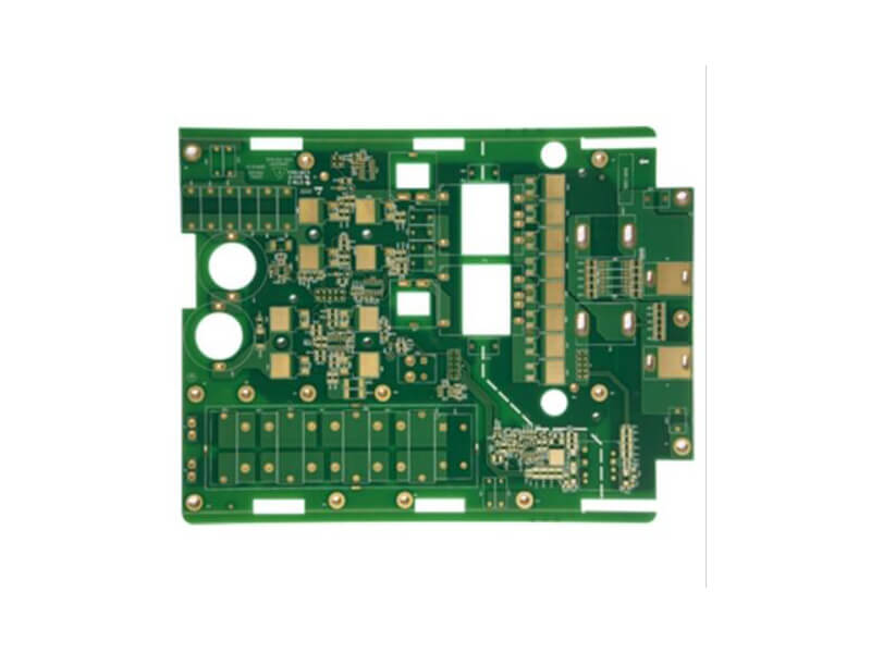
Ultra-High-Speed AI Board Design: Materials, Interconnect, and Fabrication
Accelerator boards used for large-model training, autonomous-driving compute, and HPC clusters no longer behave like ordinary motherboards. Once a serial lane runs above 100 Gbps and a single package draws several hundred watts, the laminate stops being a neutral carrier and becomes part of the electrical channel. An ultra-high-speed AI board design is judged on channel loss, power-delivery impedance, and heat removal at the same time, not on routing completeness alone.
That shift changes the order in which decisions must be frozen. Material chemistry, stackup, via architecture, fabrication process, and test coverage are now coupled: a stackup chosen purely for loss may be impossible to plate, and a via fill chosen for density may trap heat directly under the die. The sections below follow the sequence in which those constraints should be locked down.
Where Conventional FR-4 Stops Working
Standard FR-4 remains a reasonable dielectric up to roughly 5 to 10 Gbps, depending on trace length and equalization. Beyond that, insertion loss is driven mainly by the dielectric dissipation factor rather than by copper alone. Typical FR-4 sits at a Df of 0.015 to 0.020 at 10 GHz, while a purpose-built low-loss laminate lands between 0.002 and 0.004. On a 300 mm channel that difference is worth several decibels at 14 GHz and grows quickly above 25 GHz.
Bandwidth is not the only pressure. Layer counts on current accelerator carriers run from 20 to 30 layers, the channel count per package has passed a few hundred differential pairs, and the power rails must hold a tight tolerance under load steps measured in microseconds. A useful sanity check early in the project is a loss budget: if the modeled channel loss at Nyquist exceeds about 20 dB with no equalization, then one of the three variables has to move, namely material, via stub length, or routing length.
Because those variables interact, board-level decisions made for signal integrity usually have a thermal or a mechanical consequence, and the reverse is equally true. Treating the three as one problem from the start avoids the expensive late-stage rework that shows up when a stackup is frozen before the thermal path is understood.

Loss budgeting also sets the measurement plan. If the design assumes a specific dielectric constant and loss tangent, those values have to be verified on production panels, not just on the datasheet of the prepreg lot used for the first prototype.
Selecting a Low-Loss Dielectric Material
The choice of a low-loss dielectric material is governed by three numbers: Dk, Df, and the stability of both over frequency and temperature. A material with a Dk of 3.0 and a Df of 0.002 at 10 GHz is not automatically better than a Dk of 3.6 with a Df of 0.003, because Dk sets the geometry of every controlled-impedance trace and therefore determines how much routing real estate the layer budget can afford.
Two practical rules apply. First, hold Dk tolerance to plus or minus 0.05 across the panel, since a wider spread forces impedance targets to be met by etching rather than by design. Second, check the glass-weave style: loose weaves create a periodic Dk variation across a differential pair that shows up as intra-pair skew and as a resonance in the insertion-loss curve. Spread-glass or flattened-weave constructions cost more but remove a failure mode that is difficult to fix after fabrication.
Copper Foil and Conductor Loss
Above about 10 GHz the current crowds into a thin surface layer, so foil topography starts to matter as much as chemistry. Reverse-treated foil and very-low-profile foil reduce the effective path length the current travels over the treatment side and typically recover 1 to 2 dB per 100 mm at 28 GHz compared with standard foil.
The trade-off is adhesion. Low-profile copper bonds less aggressively to the dielectric, which raises the risk of delamination during reflow or at the plated barrel. A stackup that specifies very-low-profile foil on every layer should also specify a bonding treatment and a peel-strength acceptance value, otherwise the loss gain is bought with a reliability risk that shows up only after thermal cycling.
Conductor loss also depends on where the reference plane sits. Bringing a high-speed layer close to its reference plane shortens the field, widens the trace for the same impedance, and reduces both dielectric and copper loss, so changing reference-plane spacing is often cheaper than changing material.
Interconnect Architecture: 2.5D, 3D, and Any-Layer HDI
Package-level integration has moved a large share of the routing burden off the board and into the substrate, but the board still has to feed it. Silicon interposer approaches place micro-bump pitches below 40 microns, and 2.5D or 3D assemblies stack dies through through-silicon vias, which raises interconnect density by roughly an order of magnitude compared with a conventional package escape.
On the board itself, any-layer HDI construction is the usual answer when a package needs to escape several thousand pins into a limited outline. Stacked microvias allow a signal to change layers at any point, which shortens escape routes and reduces the number of long through-vias that would otherwise stub-tune the channel. The same freedom increases process risk, so stacked-via structures should be limited to two or three consecutive levels unless the fabricator has qualified deeper stacks with fill plating and confirmed the barrel integrity after thermal stress. Further detail on choosing between filled and unfilled via structures is covered in blind and buried via stack selection.
Fine-Line Fabrication: mSAP, LDI, and Pulse Plating
Line width and spacing below 30 microns cannot be produced by subtractive etching with acceptable yield, because the etch factor removes more copper than the artwork intends. Modified semi-additive processing builds the trace instead of etching it away: a thin seed layer is plated up through a patterned resist, then the seed is flash-etched. This supports 15 micron lines with 15 micron spaces on a production basis.
Imaging tolerances follow the same trend. Laser direct imaging with a 405 nm source holds plus or minus 5 microns of registration, which matters when a 40 micron pad has to land on a 40 micron capture pad across 30 layers. Plating chemistry is the third leg: pulse plating controls grain size and throws power into high-aspect-ratio holes, which sets both the conductivity of the copper and the roughness that governs conductor loss.
Thermal Management on a Power-Dense Board
Power density on an accelerator carrier routinely reaches hundreds of watts per package, and air cooling alone approaches its limit. Thermal management therefore has to start at the layout stage rather than at the enclosure. Thermal simulation run before placement identifies the hotspots, and the resulting map dictates where copper can be reduced and where it must be preserved.
Vertical heat paths are the most effective lever. A dense field of thermal vias under the die footprint, tied to internal copper planes and to a stiffener or heat spreader on the secondary side, moves heat out of the die shadow with far less resistance than spreading it laterally through the laminate. Where lateral spreading is still required, embedded copper coins or vapor chambers reduce the peak temperature by tens of degrees. The stackup question here overlaps with the general trade-offs described in EMI reduction through stackup and layout, because plane spacing serves both heat and noise.
Verification: TDR, Eye Diagrams, and AOI
Simulation narrows the design space, but manufactured hardware has to be measured. Time-domain reflectometry locates impedance discontinuities at picosecond resolution, which is precise enough to separate a connector launch from a via stub in the same channel. Eye-diagram capture on a test coupon confirms that the channel meets its mask with the intended equalization, and automated optical inspection plus X-ray review of filled vias covers the process side.
Coupon design deserves attention: the coupon should replicate the actual layer transitions, the same via structure, and the same reference-plane spacing used in the product, otherwise the measured loss will not predict the real channel. Layer-specific test structures also make it possible to isolate a dielectric problem from a plating problem when the measured loss drifts between panel lots.
Closing the Loop Between Design and Fabrication
The most reliable way to keep an accelerator program on schedule is to treat the fabricator as a design participant. Etch compensation, plating capability, and imaging registration all limit what the CAD file can ask for, and the limits differ by panel size and layer count. Signing off on a stackup before those limits are confirmed is the single most common cause of a redesign between prototype and volume build. For data-bus routing rules that complement this material, see high-frequency trace and data bus routing.
FAQ
How do I know whether to change material or change stackup first? Compute the loss budget and split it into dielectric and conductor contributions. If dielectric loss dominates at the target frequency, change the material. If via stubs or reference-plane spacing dominate, fix the stackup first, because that is usually cheaper and does not disturb the impedance targets that are already frozen.
Is any-layer HDI always required for a large accelerator package? No. It is justified when pin count, escape density, or outline area make a conventional through-via escape impossible without adding layers. If a two-level microvia stack plus a well-planned through-via layer can carry the routing, the simpler structure will have a higher yield and a shorter qualification cycle.
What should be measured on the first prototype panel? At minimum, coupon insertion loss and return loss against the simulated channel, TDR traces at each layer transition, and cross-sections of filled and stacked vias after thermal cycling. Those four data sets separate design errors from process errors before volume tooling is committed.