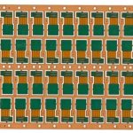
Multilayer PCB Prototyping: Inner Layer, Lamination and Drilling
A prototype build is where a design stops being a schematic and becomes an object that can be measured. The purpose of the first panels is to prove the stackup, the registration and the finish, not only the netlist, and that makes the fabrication sequence part of the engineering work rather than an administrative detail. The walkthrough below follows a six-layer board through a quick-turn shop and highlights the decisions that have to be settled before the panel is released.
What Multilayer PCB Prototyping Is For
multilayer PCB prototyping answers three separate questions. Does the circuit work, does the stackup deliver the impedance that was designed, and does the board survive the assembly process. A prototype that is built on different material, a different layer count or a different copper weight answers only the first question, which is usually the least risky of the three.
That is the argument for building the prototype on the production intent: same laminate, same prepreg types, same copper weights, same finish. The cost difference is small compared with the cost of discovering an impedance problem after the tooling is committed.
Cutting and Inner Layer Imaging
The core laminate is cut to panel size, and the copper surface is cleaned and micro-etched so the photoresist will adhere. Dry film resist is laminated under controlled temperature and pressure, then exposed through the artwork with ultraviolet light and developed, which removes the unexposed resist and leaves the pattern behind.
Etching follows, and the etch factor matters here: the process removes copper laterally as well as vertically, so a nominal 0.15 mm line comes out narrower at the top than at the base. Fabricators compensate in the artwork, but the compensation is specific to the copper thickness and the etch line, which is why a change of copper weight requires a new compensation value.
Inspection and Oxide Treatment
After stripping, the inner layers go through automated optical inspection, which compares the etched pattern with the digital image of the artwork. The inspected layers are then treated to make the copper surface suitable for bonding, traditionally with a black or brown oxide that roughens the copper and passivates it.

This treatment is easy to underestimate. A weak oxide leaves a smooth surface that bonds poorly, and a delaminated inner layer may pass every electrical test and still fail in thermal cycling. Where the design has large copper areas, the oxide must be applied so that the surface does not become brittle at the edges of the pattern.
Lamination and Registration
The stack is laid up in the order shown on the drawing, with the inner layers separated by sheets of prepreg, and the whole assembly is placed between mirror plates and pressed under vacuum. The press profile ramps temperature and pressure so that the resin flows, fills the pattern and then cures, and the cooling phase has to be controlled because the contraction of the cured resin is what determines whether the board is flat.
Registration is fixed at this stage. After pressing, the panel is drilled with X-ray targets and the tooling holes that will locate it for every subsequent step. The drill-to-copper registration budget is the sum of the lamination movement, the target drilling accuracy and the drill position tolerance, and on a fine-line design it is the parameter that decides whether the prototype is usable.
Drilling
Holes are drilled on a CNC machine with controlled entry and exit material, and the parameters are chosen to suit the hole diameter and the aspect ratio. Tool life is counted in hits, because a worn bit raises the hole wall temperature and smears the resin, which makes the subsequent plating unreliable. Burrs are removed with a dedicated deburring step rather than by brushing, which would round the copper edges and change the line width.
Plating and Copper Thickness
Plated through holes are produced in two stages: a desmear step that removes resin smear from the hole wall and prepares it for plating, and an electroless copper layer that makes the surface conductive, followed by electrolytic plating that builds the barrel and the surface copper to the specified thickness. Barrel copper of 20 to 25 micrometres is a common target for general-purpose boards, and it has to be uniform from the board surface to the centre of the barrel. Copper plating defects and their prevention covers the failure modes, which are mostly current distribution and chemistry problems.
Outer Layer Imaging and Etching
The outer layers are imaged with the same resist process, but they are normally plated rather than etched to final thickness, so the sequence is pattern plating followed by resist stripping and a short flash etch that removes the thin seed copper between features. The flash etch is deliberately short, because the plated features are already at their final width and any additional etching closes the gaps that define the fine lines.
Solder Mask, Surface Finish and Gold Fingers
Solder mask is printed, exposed and developed, then thermally cured. The finish is applied afterwards, and the choice is driven by the assembly process: an immersion finish such as ENIG for general soldering, and hard gold on gold fingers because a soft finish will not survive repeated insertion. Gold finger edges are chamfered to a controlled angle so the connector does not lift the contact springs, and the bevel dimension belongs on the fabrication drawing.
<img src="https://www.gopcba.com/wp-content/uploads/2026/09/255-1.jpg" alt="drill registration and electrical test coupon on a multilayer prototype” />
Board thickness and finish thickness both accumulate into the finger height, so the tolerance on the connector area should be specified explicitly. If the panel is a prototype for a plug-in card, it is worth asking for the bevel angle and the gold thickness to be recorded on the inspection report.
Electrical Test and Final Inspection
Bare-board electrical test checks continuity and isolation on every net, using a flying probe on prototypes and a fixture on production panels. Impedance coupons are measured and the results recorded against the stackup. Microsections are cut on a sample from each panel to verify hole wall thickness, plating quality and the dielectric spacing between layers.
For a prototype, the useful extra step is to keep one coupon and one section with the design documentation, so that a later problem can be compared with a known-good state. Multilayer PCB prototype requirements lists the inputs the fabricator needs to make the first build meaningful.
What to Specify Before the Build
Before the order is placed, the documentation should state the layer count and the sequence, the copper weight on each layer, the dielectric thickness of each prepreg and core, the impedance targets and their tolerances, the finish for each area of the board, the hard gold specification for the fingers, and the warpage limit. Anything omitted will be filled in with the shop default, which may be reasonable but is unlikely to match the electrical design exactly. PCB design guidelines for manufacturability is a useful checklist for the same review.
FAQ
Should the prototype use the production stackup? Yes wherever possible. The stackup sets the impedance and the thermal behaviour, and those are the parameters a prototype is usually built to verify. A cheaper stackup proves less than it appears to.
How long should a quick-turn prototype take? A six-layer board with standard design rules is typically a few working days from released data to shipped panels. Anything beyond the standard rules, such as blind vias or a very fine line width, adds production steps and time.
What is the most common prototype surprise? Registration and etch tolerance rather than the circuit. Fine lines come out narrower than the artwork, holes land off centre on thick copper, and impedance drifts because the dielectric thickness was not what the design assumed.