
PCB Stackup Design: Layers, Reference Planes, and Return Paths
Stackup design is where the electrical requirements of a board are translated into physical layers, and it is usually the last decision to be revisited and the first one to cause problems. How many signal layers are needed, how many planes, and in what order they are arranged determines the impedance of every controlled trace, the quality of every return path, and the emissions performance of the finished product. A deliberate PCB stackup design resolves those questions before routing begins rather than discovering them afterwards.
The competing requirements are predictable. Performance wants more planes and closer coupling; cost wants fewer layers and thicker dielectric; manufacturability wants a symmetric stack that will not warp. The stackup is the compromise between them, and it should be documented as a controlled artifact rather than left to the fabricator’s default four or six layer arrangement.
Layer Assignment and the Role of Planes
A multilayer board typically contains signal layers, power planes, and ground planes. The planes are normally solid and unsplit, because a continuous plane provides a low-impedance return path for the currents of the adjacent signal layers, and the return current follows the signal trace rather than wandering through the board.
Most signal layers should sit between a power plane and a ground plane, which makes the trace either a symmetric stripline or an asymmetric one. Buried traces of this kind are shielded by the planes above and below, so their radiation and their susceptibility are both lower than a surface trace of the same length. The outer layers carry components and a small amount of short routing, and the routing there should be kept short precisely because a microstrip on the surface radiates.
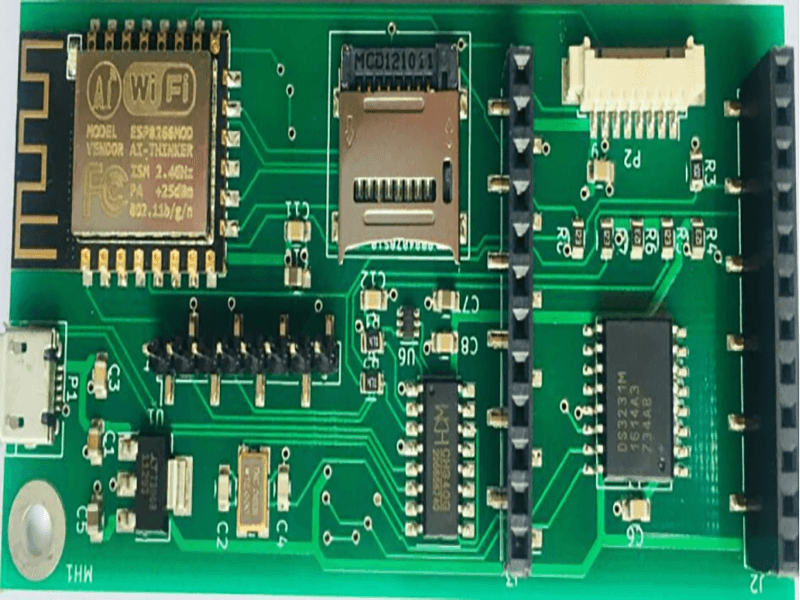
A useful check at this stage is to count the reference transitions. Each high-speed signal that changes layers also changes reference, and each of those transitions needs a return path via nearby. A stackup that forces many transitions for the fastest nets is a stackup that will be difficult to route cleanly.
Single and Multiple Power Reference Planes
Where there is only one supply voltage, the power plane can be solid and the arrangement is simple: signals are referenced to the ground plane below them and to the power plane above, and both references are continuous.
Multiple supply voltages change the picture. A multi-voltage power plane is divided into regions, and a signal routed adjacent to that layer may cross a boundary between two regions. Its return current then has no continuous path, so it must detour around the gap, which increases the loop area and therefore both emissions and susceptibility. The practical rules are to keep high-speed signals away from a split power layer wherever possible, and to route them on a layer referenced to a solid ground plane instead. The general treatment of plane division is covered in power plane splitting rules.
Multiple Ground Planes
Providing more than one ground plane is one of the cheapest performance improvements available, because an additional ground increases the number of continuous low-impedance return paths and reduces common-mode currents on the board. Where a design is struggling with radiated emissions, adding a ground layer or moving an existing layer so that it is adjacent to the noisy one often achieves more than any component change.
The coupling condition matters as much as the count. Ground and power planes should be tightly coupled to each other, and each signal layer should be tightly coupled to its adjacent reference plane. Reducing the dielectric thickness between a signal layer and its reference plane widens the trace for the same impedance, which reduces crosstalk and lowers the field that escapes the trace. In practice, the smallest dielectric thickness the fabricator can reliably produce is the right choice for signal-to-plane spacings, and the extra thickness is better spent in the core between the two reference planes.

The two planes that form the power-ground pair also act as a distributed capacitance, which helps at high frequency, and this benefit increases as the separation between them shrinks.
Routing Combinations and Reference Transitions
A routing combination is the pair of layers across which a signal travels. The best combination keeps the return current on the same reference plane: the signal changes layers, but the plane beneath it does not change, so the return current continues in the same copper.
That is not always possible on a dense board, and layer changes are unavoidable. What matters then is that the return current has a path from one reference plane to the other, which means placing a ground via or a stitching capacitor next to the signal via. Without it, the return path is forced to find its own way across the plane pair, and the resulting loop becomes an efficient radiator. Ground stitching vias placed at regular intervals between ground planes are the standard remedy, and they should also be placed around the board perimeter and near connectors.
Decoupling Capacitors and the Stackup
A decoupling capacitor can only be mounted on the outer layers, so its effectiveness is limited by how well the current can reach the device from where it sits. The trace and via connecting the capacitor to the planes form a series inductance that dominates the high-frequency performance of the part, and a capacitor connected through a narrow trace behaves far worse than its datasheet suggests.
The layout consequences are strict. Connections from a decoupling capacitor to the planes must be as short and as wide as possible, with a ground via directly adjacent to the power via so the loop area is minimized. Where a plane pair supports the highest-frequency decoupling, the thin dielectric between them is what makes the arrangement work. Because capacitor placement competes with signal routing for the same surface area, the stackup decision should include a plan for where decoupling will be placed, not just how many layers exist.
Symmetric Build and Manufacturability
Stackups must also survive the press. Copper distribution and dielectric thickness should be symmetric about the center of the board, because an asymmetric construction warps during lamination and cooling. Warpage makes assembly difficult, stresses the solder joints, and complicates the mechanical fit.
Core and prepreg selection follows the same logic: the arrangement should be buildable with standard materials, and the layer count should be chosen so that a sensible combination of cores and prepregs exists. A stackup that requires an unusual sequence of thin prepregs may be producible, but it will cost more and will be less repeatable than one that uses the fabricator’s preferred construction. How the stack interacts with emissions performance is discussed in EMI reduction through stackup and layout.
Mixed-Signal and RF Considerations
Boards that combine sensitive analog circuitry with fast digital logic need the stackup to support separation as well as routing. Digital signals should be referenced to a solid plane and kept away from the analog region, and the analog supply should have its own plane region with a defined boundary rather than sharing a split with the digital supply. Where the design includes radio frequency sections, the stackup usually needs a dedicated ground plane directly beneath the RF traces to form a controlled transmission line, which in turn constrains the layer order.
The requirements of mixed-technology boards frequently force a layer count higher than the routing alone would suggest, because the planes are needed for isolation rather than for signals. Guidance on those constraints is available in mixed-signal PCB design guidelines.
FAQ
How many ground planes does a six-layer board need? Two is the common arrangement, placed so that every signal layer is adjacent to a solid reference. A typical build is signal, ground, signal, signal, power, signal, but a better performing variant is signal, ground, signal, power, ground, signal, because it keeps the fast layers referenced to ground.
Is it acceptable to route a high-speed signal across a split power plane? It is acceptable only if the return current can follow. If the signal is referenced to a ground plane on the other side, the split in the power plane is less important, but the signal should be kept away from any plane edge or gap. Where the split is below the signal, the return path is interrupted and the loop area grows sharply.
Why does the order of the layers matter more than the number of them? Because a signal’s behavior depends on the reference plane adjacent to it, not on the total layer count. Two stackups with the same number of layers can differ substantially in emissions and impedance control depending on where the planes sit and how tightly the signal layers are coupled to them.