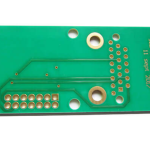
PCB Safety Spacing: Electrical and Non-Electrical Gaps
Spacing rules are the part of a design rule set that gets the least attention and causes the most avoidable rework. Most of them are not electrical at all; they exist because the fabricator needs room to etch, the assembler needs room to place and solder, and the silkscreen needs to be legible. Separating the electrical requirements from the manufacturing ones makes the numbers easier to apply, because the two categories have different reasons and different limits.
Two Categories of Spacing
electrical clearance exists to prevent breakdown, leakage or unwanted coupling between conductors at different potentials. It scales with voltage, with the contamination the board will see, and with the environment. Non-electrical spacing exists to make the board manufacturable and assemblable: the gap the etcher can resolve, the clearance the placement nozzle needs, the distance the silkscreen must keep from a pad.
The two sets are applied together, and where they disagree the larger number wins. On a low-voltage digital board the manufacturing figures usually dominate; on a board carrying mains voltage the electrical requirements are far larger and take over.
Trace to Trace Spacing
The minimum spacing between two traces, or between a trace and a pad, is set by the fabricator’s etching capability. A common production limit is 4 mil, with 6 mil being a safer standard and 10 mil a comfortable working value on boards that have the room. Spacing below the limit produces shorts and near-misses that reduce yield, and it is one of the most common reasons a design has to be modified after the first article.
Where the trace carries a higher voltage, the electrical requirement overrides the manufacturing one. Check the creepage and clearance figures for the working voltage and the pollution degree rather than extrapolating from a low-voltage design.
Drilled Holes and Annular Ring
Mechanically drilled holes have a practical minimum diameter of about 0.2 mm, and laser-drilled microvias can go down to about 4 mil. The diameter tolerance depends on the material and on the machine, and it is commonly held within 0.05 mm, which has to be allowed for when the hole is sized.
<img src="https://www.gopcba.com/wp-content/uploads/2026/06/SMT车间一角.jpg" alt="PCB safety spacing showing trace, pad and copper pullback distances” />
The pad around the hole has its own minimum. A pad width below about 0.2 mm leaves too little copper for a reliable joint and too little annular ring to survive the drill tolerance. On a dense board it is tempting to shrink the ring, and that is exactly where the fabricator will push back, because a breakout is a defect that cannot be repaired. PCB pad design standards gives the geometry for common package families, and via to trace clearance in multilayer boards covers the spacing that a via needs from unrelated copper.
Pad to Pad Spacing
The gap between adjacent pads is limited by the same etching process as trace spacing, and about 0.2 mm is a widely used minimum. On fine-pitch packages the pads are already at that limit, which is why the solder mask and the stencil apertures become the controlling features rather than the copper itself.
Where two pads belong to nets at different potentials, the electrical requirement may be larger than the process minimum, and the gap also has to be wide enough for the solder mask dam between them to survive. A dam that is too narrow will not hold, and the resulting bridge is a defect that appears only after assembly.
Copper to Board Edge
Copper must be pulled back from the routed edge by at least about 0.3 mm. The reasons are mechanical rather than electrical: a cut exposes the laminate, and copper that reaches the edge can burr, can be damaged by the router, and can short against an enclosure or a neighbouring board.
A large copper pour is usually inset further, and 20 mil, or about 0.5 mm, is a common figure. This copper pullback is normally implemented with a keepout on the outline layer combined with a pour clearance, which is more robust than drawing the pour by hand and hoping it stays clear. The inset also reduces the fringing field at the board perimeter, which is why it appears in EMC guidance as well as in manufacturing rules.
<img src="https://www.gopcba.com/wp-content/uploads/2026/08/flexible-pcb-assembly-process.jpg.webp" alt="silkscreen clearance and pad spacing on a dense PCB layout” />
Silkscreen Character Size and Spacing
silkscreen clearance is a non-electrical rule with a practical basis. Characters drawn too small print as an illegible smear, so a minimum height of about 30 mil with a 5 mil stroke is a common working figure, and 36 mil characters with a 6 mil stroke are easier to read on a dense board.
The marking must not overlap a pad. Solder does not wet silkscreen ink, so a designator printed over a pad reduces the solderable area and can interfere with the stencil. Most fabricators ask for about 8 mil between the silkscreen and the pad edge, and 4 mil is the practical floor where space is tight. Where the ink does overlap, the fabricator will clip it, which is acceptable for the board but leaves the marking truncated, so it is better to move the text.
Mechanical Clearance in Three Dimensions
The spacing rules that are easiest to overlook are the vertical ones. Two components can be electrically and horizontally clear and still conflict in height, either with each other or with the enclosure. The clearance has to be checked against the real body dimensions, including the tolerance on the part and on the placement, not against the courtyard in the library.
The same applies between the assembled board and the product housing. A connector that needs a cable bend radius, a shield can that must not touch a metal boss, and a battery that expands slightly with age all need space that the layout has to reserve. Board outline and mounting design covers how those clearances are established with the mechanical design.
Setting the Numbers for a Project
It also helps to know which rules are negotiable and which are not. Trace spacing can sometimes be tightened with the fabricator’s agreement and a yield penalty. An annular ring that is too small cannot be rescued at all, and a silkscreen marking over a pad will simply be clipped. Prioritise the space budget accordingly.
The sensible approach is to take the manufacturing minima from the fabricator, add the electrical requirements for the highest voltage on the board, and then apply a design rule set that combines them. Where the two conflict badly, the answer is usually a layout change rather than a relaxation of either.
Record the numbers in the fabrication drawing and in the design rules so that they survive the next revision. A design that meets its spacing rules by accident, because the layout happened to have room, will not survive a change of enclosure or a cost reduction on the board area.
FAQ
What is the minimum trace spacing? About 4 mil on a standard process, with 6 mil a safer choice and 10 mil comfortable. Anything below the fabricator’s published minimum requires their agreement.
How much copper pullback is needed at the board edge? A minimum of about 0.3 mm, with 0.5 mm common for a large pour. The larger figure is also better for edge radiation.
Can silkscreen touch a pad? It should not. The ink is not solderable and reduces the area available for the joint. Keep about 8 mil of clearance, and move the marking rather than relying on the fabricator to clip it.