PCB Testing and Inspection Methods Explained
Every board that leaves a fabrication line has been inspected many times, and every board that leaves an assembly line has been tested in ways that are invisible to the customer. The combination of inspection and pcb testing is what turns a manufacturing process into a qualified one, and the choice of which checks to apply is an engineering decision driven by feature size, volume and the cost of a field failure.
Inspection Is Not the Same as Test
Inspection looks for defects that can be seen or measured: a short, a missing pad, a misregistered layer, a solder bridge. Test applies a stimulus and measures a response, which means it can find a fault that has no visible signature at all, such as a cracked barrel inside a plated hole or a wrong value component that was placed correctly.
The distinction matters because the two methods fail in different ways. Inspection is fast and cheap per board but limited by resolution and by what the camera can see. Test is slower and requires tooling, but it reports on the electrical reality of the assembly rather than on its appearance. A production plan needs both.
Bare Board Electrical Test and Continuity
The first test a board sees is bare board electrical test, sometimes called flying probe test on prototypes and fixture test at volume. A flying probe moves two or more probes over the board under programme control, checking continuity on every net and isolation between adjacent nets. It requires no tooling, which makes it the natural choice for prototypes and small batches.
At volume, a dedicated fixture with fixed probes performs the same checks far faster. The programme verifies that every net is connected to what the design intended and that nothing is connected that should not be, which catches open traces, shorts, and plated barrels that failed during electroplating. Boards that fail are marked and scrapped before any components are added to them.
<img src="https://www.gopcba.com/wp-content/uploads/2024/09/tupian4.png" alt="Automated optical inspection of an assembled PCB” />
Automated Optical Inspection
After assembly, automated optical inspection compares the board against a reference image or against the design data. It finds missing components, misaligned parts, tombstoned passives, insufficient solder and bridges, and it does so at a speed that no manual inspection can match. Modern systems combine two dimensional colour imaging with laser based three dimensional measurement of the solder joints.
The technique has one structural limitation: it can only see what is exposed. A ball grid array or a chip scale package hides its joints entirely, and a fillet that looks correct might cover a joint that never wetted. Optical inspection therefore covers the visible population and is complemented by X-ray for the rest.
X-Ray and Acoustic Inspection
X-ray inspection transmits through the assembly and images the dense metal inside it, which makes it the standard method for verifying area array solder joints and for checking the integrity of buried vias and their registration. Two dimensional systems show the joint density; computed tomography reconstructs slices through the package to reveal voids and cracks in three dimensions.
For interface layers and for delamination between laminate plies, ultrasonic scanning is used instead, because sound reflects from a layer that has separated where X-ray would show nothing unusual. The choice between the two techniques follows from what is being looked for: metal geometry for X-ray, layer bonding for ultrasound.
In-Circuit and Flying Probe Assembly Test
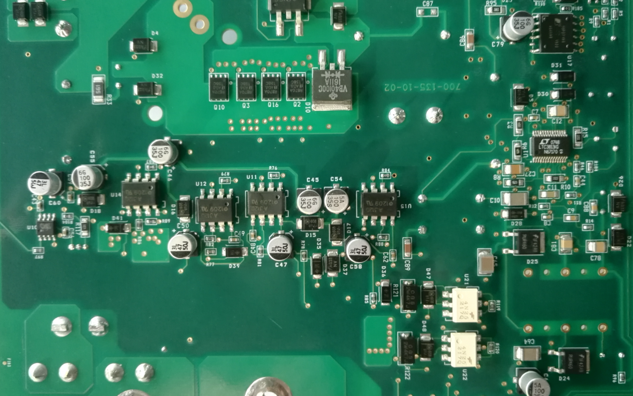
Once components are fitted, in-circuit test checks each part individually through probe access on the assembled board. It verifies values, orientations and continuity, and because it measures components one at a time, a failure can be identified without the design having to work as a whole. It needs a fixture and a programme, so it is economical only at volume.
A flying probe system provides a similar measurement without the fixture, which suits low and medium volumes and designs that are still changing. It is slower per board, since the probes move serially, but it can be reprogrammed in minutes and it does not become obsolete when the layout changes. For designs that are sensitive to probe loading, the probe capacitance and resistance have to be taken into account.
Functional and Environmental Testing
Functional test powers the assembly and exercises its intended behaviour. It is the most convincing form of verification, because it demonstrates that the product functions rather than that its parts are present. Its weakness is diagnostic: when it fails, it usually reports a symptom rather than a cause, which is why it is normally preceded by in-circuit test on high volume builds.
Environmental testing then establishes the operating envelope. Thermal cycling subjects the assembly to repeated expansion and contraction, which is the condition that cracks plated barrels and solder joints. Humidity and salt spray testing address corrosion, and vibration testing addresses mechanical attachment. These are qualification tests rather than production tests, so they are applied to samples rather than to every unit.
Impedance, Microsection and Solderability
For controlled impedance boards, time domain reflectometry measures the characteristic impedance of the test coupons on each panel. The results confirm that the stackup thickness and trace geometry are inside tolerance, and they are the only practical way to verify impedance before assembly. A microsection cut through a coupon reveals plating thickness, layer registration and copper quality, and it is used both for process qualification and for failure analysis.
Solderability testing confirms that the finish is actually wettable, which matters most for boards that have been stored for a long time or that use an organic finish with a limited shelf life. Ionic contamination testing measures residues left by the assembly process, since a board can pass every electrical check and still fail in the field because a conductive residue created an unintended leakage path. The design practices that make these checks effective are covered in PCB design quality characteristics.
Building the Test Plan
A practical plan layers the methods by cost. Bare board electrical test on every board; optical inspection after assembly; X-ray on the area array packages if the volume supports it; in-circuit or flying probe test on production boards; functional test on a sample or on every unit depending on the consequence of failure. Each layer catches what the one before it cannot.
The plan also has to consider what happens when a test fails. A repair station with proper tooling, a documented rework procedure and a re-test step is part of the test plan, not an afterthought, and a board that is reworked must be inspected again by the same method that failed it. The layout decisions that make probing possible are described in design guidelines for manufacturability.
FAQ
Is X-ray inspection necessary on every build? No. It is essential where ball grid arrays or other area array packages are present, and unnecessary where all joints are visible. Applying it selectively keeps inspection cost proportional to the risk it removes.
How much does an in-circuit test fixture add to the project? The fixture and programme can cost more than twelve thousand dollars, which is why the method is reserved for stable, high volume designs. Flying probe testing covers the same nets without that tooling cost at a higher cost per board.
Can a board pass all tests and still fail in the field? Yes. Production tests verify the assembly, not the design margin. A marginal design will pass every inspection step and still fail under temperature or aging, which is why qualification testing is done on samples, as described in placement order and pad positioning.