5 Key Stages of PCB Prototype Manufacturing
Almost everyone who works with electronics knows what a printed circuit board is, and far fewer know how one is actually built. Modern boards are constructed with a pattern plating process, in which copper is plated onto the areas that will become conductors and the rest of the copper is removed. The stages that follow are broadly the same across manufacturers, even though the equipment, the drilling method and the test strategy differ. This article walks through the five stages that matter most in PCB prototype manufacturing, with the etching step in the detail it deserves.
How a board is constructed
The starting point is a substrate clad with copper on one or both faces. A temporary mask defines the pattern, and the exposed copper is either built up or etched away depending on the process. Because the pattern has to be protected while everything else is removed, the sequence of imaging, plating, etching and stripping is what turns a blank panel into a circuit. Manufacturers vary the details, particularly in component mounting technology and test method, and they run automated drilling, plating and profiling equipment for volume. The main stages, however, do not change.
Stage one: the etching process
Etching removes the unwanted copper from the panel using a temporary mask, leaving the required conductors behind. Production lines use an aggressive ammonia-based solution or ferric chloride or hydrochloric acid; all three are inexpensive and widely available. For a single prototype made by hand, the transfer method is still common, and it runs in eight steps.
Design the board in whichever layout tool is available, then print the artwork onto transfer paper with the design on the glossy face. Clean the copper board by sanding it so the surface is rough enough to hold the toner; wear gloves during this step, because skin oils transfer to both the board and the paper and prevent adhesion, and make sure the abrasive reaches every edge. Wipe the board with water and alcohol to remove loose copper particles, then let it dry completely. Cut the printed design to size and place it face down on the copper, then pass the sandwich through a laminator several times until it is hot. Transfer the hot board to a cold water bath and agitate it briefly so the paper floats away from the copper. Place the board in the etching solution and agitate it for roughly half an hour, which dissolves the unwanted copper around the pattern. Once the excess copper is gone, dry the board and wipe it with alcohol to remove the ink that carried the design. The board is now ready to be drilled with the appropriate bits.
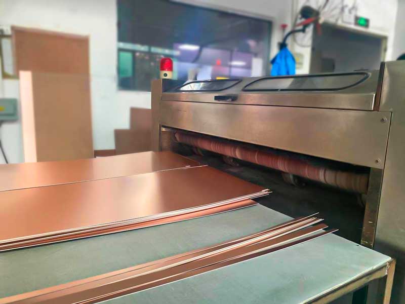
Etching on a production line
Volume production replaces the hand method with a conveyorised spray etcher, but the physics are the same. Etchant concentration, temperature, spray pressure and conveyor speed set the etch rate, and the dissolved copper load has to be monitored because it changes that rate over time. The result is judged by line width consistency and by undercut at the trace edges, which is why the artwork is compensated before imaging and why the line width is measured across the panel rather than at one point. The design and fabrication review should confirm that the minimum spacing in the layout matches what the etching process can actually hold.
Stage two: stripping
After etching, the copper that remains is still covered by the plated resist that protected it, usually a tin or tin-lead layer. Stripping removes that metal without attacking the copper underneath. Nitric acid is effective for the purpose: it dissolves the tin while leaving the copper conductor intact. What remains is a clean, well-defined copper pattern, and the panel moves on to the next stage ready for its permanent coating. Incomplete stripping shows up as patches of metal on the traces and is one of the defects an operator looks for before the board is coated.
Stage three: solder mask
The solder mask coats the areas of the board that will not be soldered. Its purpose is not cosmetic. Without it, molten solder can spread along a trace and form a bridge to an adjacent lead, and a bridge between two fine-pitch pins is a short. The mask also protects the copper from oxidation and from handling damage, and it defines the openings that keep the pads clean for soldering. Mask thickness, cure schedule and adhesion to the laminate all matter, because a mask that lifts after reflow exposes copper and creates a defect that appears later rather than at inspection.
Stage four: electrical test
Once the board is fabricated, it has to be tested for continuity and insulation before anything is assembled onto it. The manufacturer verifies that the board performs as the netlist expects, checking every net for opens and every pair of neighbouring nets for shorts. Volume production normally uses automated test equipment with a bed of nails fixture, while prototypes and small batches are usually tested with a flying probe test, which needs no fixture and can reach very fine pitch. Catching an open at this stage costs a repair; catching it after assembly costs the components as well. The basics of a circuit board explain why the netlist, not the visual appearance, is the reference for this check.

Stage five: component assembly
The final stage places components on the board and forms the electrical and mechanical joints. Through-hole technology inserts leads into drilled holes and solders them on the far side; surface-mount technology places parts on pads and reflows the whole assembly in one pass. Both rely on molten solder for the connection, and both depend on the pad geometry and the placement accuracy of the machine. Where the two technologies are mixed, the sequence has to be planned so that the second soldering operation does not disturb the joints made by the first, which is a question of placement order and pad positioning rather than of equipment capability.
Drilling, imaging and plating around the five stages
Three operations sit between the stages described above and are easy to overlook when the process is summarised. Imaging transfers the artwork onto the panel with a photosensitive film; exposure and development leave resist only where copper must survive or be added. Drilling creates the holes that will connect the layers, and its parameters decide whether the barrel can be plated evenly, which is why the hole diameter has to be checked against the board thickness. Plating then builds copper inside those holes and, in a pattern plating process, on the conductor pattern at the same time. A defect introduced in any of the three will usually be detected at electrical test, but it will have been created much earlier, and the design and fabrication review is where the drill and plating limits are normally confirmed. None of this is visible in the finished product, which is why the process is worth understanding rather than assuming.
FAQ
Do all manufacturers follow the same five stages? The stages are the same, but the equipment, the etch chemistry and the test method vary. A shop that specialises in prototypes may use hand or slow-line processes where a volume shop uses conveyorised equipment, and the choice affects lead time more than the sequence.
Why is stripping a separate stage from etching? Etching removes copper that is not protected, while stripping removes the metal that protected the copper. The two use different chemistries and attack different materials, so they cannot be combined without damaging the conductors.
Is electrical test always done before assembly? It should be, because a bare board defect is cheap to repair and an assembled board defect is not. Where a board is not tested, the risk is carried into the assembly line and any failure is far more expensive to resolve.