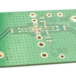
Layer Stack-Up Strategy for EMI Shielding
Most engineers treat the layer stack as a mechanical necessity, but on a fast board it is also the main electromagnetic component. The planes, their spacing and their order decide how much energy leaves the board, how clean the power delivery network is, and how susceptible the design is to fields arriving from outside. A stack-up chosen for EMI shielding costs no more than one chosen at random, provided the decision is made before routing.
The notes below explain the mechanism, then walk through the four-layer and six-layer options that are worth considering.
The Stack-Up as an EMI Tool
Every current that leaves a driver returns to it. The route that return current takes depends on the reference plane directly beneath the trace, and the area enclosed by the outgoing and returning currents sets how efficiently the loop radiates. A signal layer adjacent to a solid ground plane keeps that loop small; a signal layer isolated from any plane lets the return current wander.
Good layer stack-up therefore suppresses emissions at the source instead of shielding them afterwards. A shield can adds cost, weight and assembly steps, and it only works if the underlying loop area is already reasonable. The stack does the first ninety percent of the work, and the remaining tuning is described in the layout measures for EMI reduction.

The Power Plane Is a Distributed Capacitor
A power plane and the adjacent ground plane form a parallel-plate capacitor. With 6 mil of dielectric between them and FR-4 as the material, the equivalent capacitance is roughly 75 pF per square inch. Reducing the spacing raises the capacitance in proportion, so a 3 mil core doubles it.
That capacitance supplies the high-frequency energy a fast driver needs before the discrete decoupling capacitors can respond, and its low inductance is what suppresses the transient voltage that drives common-mode current. The plane pair should be wide, unbroken and as close together as the fabrication tolerance allows.
Four-Layer Options
The conventional four-layer stack puts the two signal layers outside and power and ground inside. It is cheap and easy to build, but on a 62 mil board the spacing between the power and ground planes is large, which weakens the distributed capacitance and reduces the shielding benefit.
Two alternatives improve on it when component density is low enough to leave copper area free. The better one places ground on both outer layers and runs signals and power on the inner layers, using wide traces for the power. Signals then reference the outer ground planes directly, so the loop area is minimal and the impedance is easy to control.
Six-Layer Options
A six-layer board becomes worthwhile when a four-layer board runs out of routing space. Not every six-layer arrangement is an improvement, though. Putting power on layer two and ground on layer five gives good impedance control for signals but leaves the power plane with high spreading inductance, which is poor for common-mode emissions.
Putting power on layer three and ground on layer four is better for the power distribution network, but the outer layers then have weak shielding, so differential-mode emissions rise. That is acceptable when the outer layers carry few, short traces, and when unused copper on the outer layers is flooded and tied to ground at intervals shorter than one twentieth of a wavelength. These measures work together with the general suppression principles rather than replacing them.

Where the Signal Layers Should Sit
Signals belong on layers that touch a plane. Microstrip on an outer layer with ground beneath it is the cheapest controlled-impedance structure, while stripline between two planes gives the best isolation because the field is fully contained. The cost of stripline is routing access, since every connection has to reach the inner layer through a via.
When several signal layers exist, pair each one with a plane rather than stacking signal layers together. Two signal layers separated only by prepreg couple strongly to each other, and no amount of impedance control will remove that coupling once it has been designed in.
Copper Islands and Stitching
Plane copper that is not connected is not a plane. Islands on a power or ground layer must be stitched together with vias so that direct current and low-frequency signal return path behaviour remains continuous, and the stitching density has to be high enough that the islands behave as one conductor at the frequencies of interest.
Flooding unused areas and tying them to ground helps suppress differential-mode radiation, but the connections must be frequent. A flood tied down only at its corners presents a long, narrow structure that can itself resonate.
Choose the Stack for the Rise Time You Have
The plane spacing that is adequate depends on the edge rate. For parts with rise times of one to three nanoseconds, ordinary 3 to 6 mil plane spacing on FR-4 is sufficient: it supplies enough high-frequency energy and keeps the transient voltage low enough that common-mode current stays small.
Devices with rise times of 100 to 300 picoseconds need closer plane pairs and, at the extreme, a thinner dielectric with higher permittivity instead of FR-4. That is a materials decision as much as a stack decision, and it should be taken with the loss budget in hand rather than after the layout is complete.
How the Stack Affects Cable Radiation
Every cable attached to the board behaves as an antenna driven by the common-mode voltage that appears on the ground plane. That voltage is produced by transient currents flowing through the plane inductance, so the smaller the plane impedance, the smaller the drive available to the cable. A tight power and ground plane pair, stitched frequently, keeps the impedance low across the band where the cable radiates most efficiently.
If the ground plane is split, or if a signal layer sits far from its reference, the common-mode voltage rises and the cable radiates a correspondingly larger field. The practical measures follow from the mechanism: keep the ground plane continuous under every connector, tie the connector shell to that plane with several vias placed close to the pins, keep the plane pair spacing small near the connector where the transient current is largest, and add a common-mode choke or a ferrite at the cable exit. None of these steps requires extra layers, and together they often recover several decibels of margin at the worst frequency. Consult the ground routing and power planning rules when the connector area is also the densest part of the layout.
FAQ
Is it worth adding a separate ground layer on a six-layer board? Usually yes. Two plane layers let you place a ground adjacent to each signal layer, which is the property that actually reduces emissions. If only one plane layer is available, keep the signals on the layers closest to it.
How far apart should stitching vias be? A working rule is one twentieth of a wavelength at the highest frequency of concern, which also keeps the plane impedance low. At 1 GHz that is about 15 mm; at 5 GHz it falls to about 3 mm.
Can a two-layer board be made quiet? It can be quiet enough for many products if the ground is flooded on the bottom layer, the fast signals stay on top with short direct returns, and the power traces are wide and heavily decoupled. It will not match a four-layer board, but the gap is smaller than most people expect.