High-Speed PCB Via Design: Parasitics and Sizing
On a fast board, the via is usually the weakest electrical element in the interconnect. It is short, it is cheap, and it is invisible on the schematic, yet it adds capacitance to the trace, inductance to the return path, and a stub that behaves differently at every frequency. High-speed designs live or die on how well via design is controlled, because a trace that is perfectly matched through three inches of copper can still fail at the point where it changes layers.
The three parts of a via
Every via is built from three features: the hole itself, the pad area around the hole, and the clearance in the power or ground layer, often called the antipad. The barrel of the hole is plated by chemical deposition, which builds a conductive layer on the cylindrical wall and connects the copper foils of the layers that must be joined. The pads on the top and bottom surfaces take the shape of a normal land, and they may or may not connect to the outer-layer traces.
A via therefore performs two jobs. Electrically it connects nets that need to be joined; mechanically it can also locate or retain a component. The distinction matters during review, because a via placed for mechanical reasons still behaves as an electrical discontinuity.
Through, blind, and buried vias
Through vias pass through the entire board and are used for internal interconnection or as component mounting and locating holes. Because they are easy to produce and inexpensive, most printed circuit boards still use them exclusively.
A blind via starts at the top or bottom surface and stops inside the board, connecting an outer layer to an inner layer without passing through. A buried via connects inner layers only and never reaches either surface. Both are formed before lamination using the same drilling and plating processes, and a single stackup may contain several overlapping inner layers built in this way.
The depth-to-diameter relationship is what makes these structures practical. Blind and buried vias are only manufacturable while the aspect ratio stays inside the process window, which is why their diameter shrinks as the layer count grows.
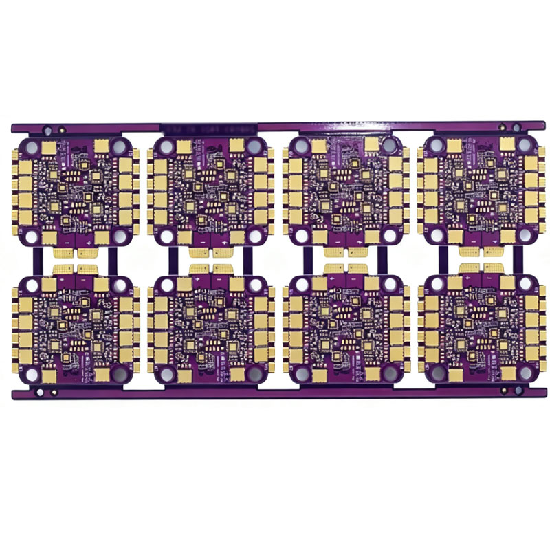
A blind via is judged by its depth, not by its diameter. Two vias of the same finished size can have completely different electrical behaviour once the drilled depth differs.
Parasitic capacitance
A via presents capacitance to the ground plane around it. If the clearance diameter in the plane is D2, the pad diameter is D1, the board thickness is T, and the dielectric constant of the base material is e, the parasitic capacitance is approximately C = 1.41 e T D1 / (D2 – D1). The expression is worth reading rather than memorising: capacitance grows with board thickness and with pad diameter, and shrinks as the clearance around the pad grows.
The electrical effect is a longer rise time. A via that adds capacitance to a fast edge slows that edge down, which reduces timing margin and, in the extreme, converts a clean digital signal into a soft one. Smaller capacitance means a smaller penalty, so the pad diameter is the first parameter to question.
Parasitic inductance
A via also has series inductance, and in high-speed digital circuits its cost usually exceeds the cost of the capacitance. The inductance of a via with length h and drilled diameter d is approximately L = 5.08 h [ ln(4h/d) + 1 ]. The diameter appears inside a logarithm, so it barely matters; the length h is the dominant term and it appears both directly and inside the logarithm.
The damage is indirect. Series inductance in the path between a decoupling capacitor and the device it serves weakens that capacitor exactly when it is needed, which degrades the filtering of the whole power distribution network. The practical conclusion is that the vertical distance between a supply pin, its via, and its capacitor is far more important than the via diameter.
Why non-through vias pay off
Blind and buried vias reduce board size and weight, allow fewer layers, and improve electromagnetic compatibility, because they remove the long plated barrels that punch through every plane on the board. Through vias consume routing space, obstruct inner-layer routing, and break the impedance of power and ground planes where they pass through in groups. Mechanical drilling of through holes also costs far more machine time than the laser processes used for small blind structures.
The electrical gain is measurable. A small blind via around 0.3 mm in diameter can present roughly one tenth of the parasitic parameters of a conventional through via, which improves reliability and leaves more room on the board. That space can be used for shielding, for partial shielding of critical nets on inner layers, and for easier fanout of high-density packages such as BGAs, where shorter escapes directly improve timing. The trade-off is that thin boards and careful aspect ratio control are prerequisites, since a growing aspect ratio reduces plating reliability.
Choosing via sizes
On ordinary boards the parasitics are mild and standard sizes work well. For one to four layer designs, a via of about 0.36 mm drill, 0.61 mm pad, and 1.02 mm clearance is a good default, while supply, ground, and clock nets can use a larger 0.41 mm drill with a 0.81 mm pad and a 1.32 mm clearance.
For high-speed multilayer designs, a 0.25 mm drill with a 0.51 mm pad and a 0.91 mm clearance suits ordinary density, and 0.20 mm with a 0.46 mm pad and 0.86 mm clearance suits high density, where a blind via may be a better answer still. Power and ground vias should be larger rather than smaller, to lower impedance. The clearance should be as wide as the via density allows, and a common starting point is a pad diameter about 0.41 mm larger than the clearance diameter.
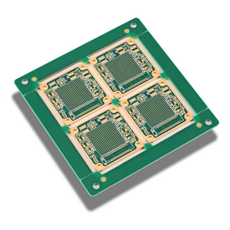
Smaller vias are not automatically better. Below a certain diameter the plating process, not the electrical requirement, sets the limit.
Layout rules around vias
Four habits cover most of the risk. Keep signal traces on one layer wherever possible, so the number of layer changes falls. Use a thinner board when the stackup allows it, since both parasitic terms scale with thickness. Route the via for a supply or ground pin as close as possible to that pin, with the connecting trace as short and as wide as the layout permits. Finally, place ground vias next to every via that carries a signal from one layer to another, so the return current has a short path to follow.
The remaining decisions are trade-offs between cost and signal quality. Smaller vias free routing space and reduce capacitance, which favours high-speed nets, but they cost more to drill and plate and they cannot be reduced indefinitely. Balancing the two is the actual engineering task, and the stackup choice is where it is settled. Our guides to blind and buried via stack selection, via in pad versus plated through, and via to trace clearance in multilayers cover the fabrication side of those choices.
FAQ
Which via parameter matters most at high speed? Length. Inductance rises almost linearly with the drilled depth, while diameter barely changes it, so a thin board is worth more than a smaller hole.
Should every signal via have a ground via beside it? Every via that changes layers carries a return current that must change layers too. Providing a nearby ground via gives that current a defined path instead of letting it find one through the plane gaps.
When is a blind via worth the extra cost? When the through via would block inner-layer routing, break a reference plane, or add more stub length than the timing budget allows. Below that threshold a through via does the same job for less money.