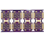
PCB Layer Structure and What Each Layer Does
A layer in a circuit board layout is not the same thing as a layer in the physical board. The design file carries many layers, some of which become copper, some of which become coatings and some of which exist only to instruct the fabricator. Understanding what each one does is what allows a design to be read and corrected by someone other than its author.
Copper Layers
The copper layers carry the circuit. On a double sided board there are two, one on each face, and on a multilayer board there are as many as the stackup requires. Each copper layer is a separate image that is etched independently.
In a multilayer stack the copper layers are assigned functions: some carry signals, some are planes connected to a supply or to ground. That assignment is not fixed by the material, it is decided by the designer, and it determines the electrical behaviour of the whole board. Our layer assignment article describes how the decision is made.
Signal Layers
A signal layer carries the traces that connect components. On a well designed board each signal layer has a plane adjacent to it, which gives every trace a nearby return path and a defined impedance.
Where two signal layers sit next to each other with no plane between them, the traces couple into one another and neither has a controlled reference. That arrangement is sometimes forced by cost, but it should be a deliberate compromise rather than an accident of the stackup. Our impedance continuity notes describe the resulting problems.
Plane Layers
A plane is a copper layer that covers most of the board area and is connected to one net, usually ground or a supply. Its purpose is to provide a low impedance return path and, where it is adjacent to another plane, to form a distributed capacitance that supplies fast current to the devices above it.
Planes are usually drawn as a filled area with clearances around the vias and pads that must not connect to them. How those clearances are shaped matters at high frequency, because a large antipad creates a gap in the current path. The plane is therefore not a passive background but a designed structure. Our EMC design techniques article describes how that structure affects emissions.
<img src="https://www.gopcba.com/wp-content/uploads/2026/09/222-1.jpg" alt="silkscreen and solder mask over copper on a finished board” />
Solder Mask
The solder mask is the coating that covers the copper except at the pads. It prevents solder from bridging between adjacent joints during assembly and protects the copper from contamination and oxidation.
Mask openings are larger than the pads they expose, which creates a web of mask between adjacent features. Where that web becomes too narrow it breaks down during assembly and allows bridging, so mask geometry imposes its own spacing rule. The colour of the mask is cosmetic, but the choice of matte or gloss affects inspection, because a glossy surface reflects light into the camera.
Silkscreen
The silkscreen layer carries the printed markings: reference designators, polarity indicators, connector labels and the product identification. It is printed on top of the mask and has no electrical function, but it has a substantial practical one.
Silkscreen should never overlap a pad, because the ink is not designed to be soldered through and its presence impairs the joint. Keeping the legend readable at the finished size is the other constraint, which becomes difficult on small boards and forces the designer to prioritise which markings are essential. Our routing techniques article covers the checks to run before release.
Paste and Drill Layers
The paste layer is not part of the board. It is the data used to cut the stencil, and it defines where solder paste will be printed. It differs from the mask layer in being slightly smaller than the pad on most features, for reasons that belong to the printing process.
The drill layer is similarly a set of instructions rather than a physical layer. It lists the hole sizes and their positions, and it is used to program the drilling machine. It must be consistent with the copper layers, because a pad without a hole or a hole without a pad is a defect that no amount of inspection will correct. Our pad and hole size article describes how those dimensions are chosen.
Mechanical and Documentation Layers
The board outline defines the physical extent of the board, and it must be a closed contour on a layer that the fabricator expects. Where the outline is open, duplicated or drawn on the wrong layer, the design is returned for clarification.
Documentation layers, such as a fabrication drawing or an assembly drawing, carry the information that cannot be expressed in copper: the stackup, the surface finish, the tolerances and the assembly notes. They accompany the design rather than becoming part of the board. Our design release checklist describes what belongs in each.
Why Layer Discipline Matters
A design that uses layers consistently is easier to review, easier to modify and harder to break. A design that draws copper on a documentation layer, or a legend on a paste layer, produces a board that differs from the drawing and a review that cannot catch it.
The discipline is simple: copper layers carry copper, mask and silkscreen carry their own coatings, paste and drill carry instructions, and drawings carry requirements. Keeping each layer to its purpose costs nothing and is what makes the whole design legible. Our PCB types article describes how many layers a given product is likely to need.
Plane Layer Details That Matter
A plane layer looks like a solid sheet in the layout, and it is almost never one. It is perforated by antipads around every via that must not connect to it, and those openings interrupt the current path beneath the traces above.
The shape and size of the antipads therefore affect the electrical behaviour of the plane, not just its manufacturability. A large antipad creates a wide gap, and a row of them creates a barrier. Keeping them as small as the drill tolerance allows, and breaking up long rows of vias, preserves the reference that the plane exists to provide.
Layer Count and Its Consequences
Each added layer gives the designer more room, and it also adds a lamination interface, a drilling step and a yield risk. The decision is usually made once, early, and it is expensive to revisit afterwards.
The count should follow from the number of nets that must cross, the number of supply rails that need their own reference, and the impedance requirements of the fastest interfaces. Where those three are modest, a four layer board is often enough. Where they are not, the count rises quickly and the cost rises with it.
FAQ
Does a four layer board have four copper layers? Yes. The count refers to copper layers. The solder mask and silkscreen are additional coatings rather than numbered layers.
Can silkscreen be removed to save cost? It can, and the saving is small. Removing it also removes the assembly information, which costs more in the assembly stage than it saves in fabrication.
What happens if the paste layer is wrong? The stencil is cut to the wrong shape, and the solder volume on the affected pads will be wrong. It is a fabrication error that first appears as a soldering defect.
Why do mask openings differ from pads? Because the mask must fully clear the pad and still leave a web between adjacent features. The registration tolerance is why the opening is larger.
Which layer carries the board outline? A dedicated mechanical or outline layer, defined as a closed contour. Its name depends on the design tool, and the requirement should be stated to the fabricator.