HDI PCB vs Standard PCB: Differences and Selection
Not every board has to be built the same way, and the gap between a conventional board and a high density interconnect board has widened to the point where they are almost different products. Choosing between them is not a matter of prestige but of geometry: if the component pitch and the pin count fit inside the routing rules of an ordinary board, an HDI PCB buys nothing and costs a great deal.
What a Standard Board Provides
A standard PCB is the conventional laminate construction that has been in volume production for decades. It typically carries one to eight layers, with some designs reaching twelve, and it uses ordinary through holes to connect every layer. Trace width and spacing are relatively coarse, which keeps etching predictable and yields high, and the base material is a general purpose epoxy glass laminate.
The advantages are all economic and logistical. Manufacturing cost is lower because the process steps are simple and the tooling is common. Turnaround is shorter because the design can enter any production line. Reliability is well characterised because the construction has been qualified by decades of field data across consumer, industrial and automotive programs.
What Changes on an HDI Board
A high density interconnect board is designed to fit more function into a smaller area, and it does so with finer features and denser interconnect. Layer counts of six to twenty or more are normal, with microvias formed by laser drilling and with blind and buried vias used to reach inner layers without consuming space on every layer. High performance laminates are often used to keep loss low.
The result is a smaller board with shorter signal paths. Shorter paths mean less inductance and capacitance in the interconnect, which improves signal integrity and reduces the radiated coupling that shows up as electromagnetic interference. The advanced materials and tighter process control also raise durability, which is why the technology is common in products where a failure is not an option.
Comparing the Two Directly
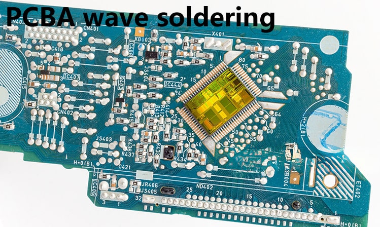
The layer count is the first visible difference: one to twelve for a standard board against six to twenty or more for HDI. The second is feature size, since a standard board uses noticeably wider traces and larger spacing than an HDI board. The third is the interconnect itself, with through holes on the conventional board and a mix of microvias, blind vias and buried vias on the HDI board.
The fourth difference is the material. A standard board uses an ordinary FR-4 class laminate, while an HDI board often moves to a low loss laminate where the dielectric constant and loss tangent have to hold over a wide frequency range. Cost follows directly from those choices: HDI is more expensive per unit area, and the gap widens as the layer count rises. A useful way to frame the comparison is that the standard PCB optimises for cost per square metre, while the HDI board optimises for function per square centimetre.
When a Standard Board Is the Right Answer
Choose a conventional board when the function is basic and does not need advanced features. A control board for an appliance, a power supply, a lighting driver or an industrial interface usually falls into this category. If the budget is tight and the application does not demand miniaturisation or high speed performance, the conventional board is both cheaper and faster to obtain.
Prototyping and small batch production also favour it. Because the process is common, a prototype can be turned around in days and the same data can be released to any fabricator. The design rules are well understood by every engineer, which reduces the chance that an unusual construction delays the build.
<img src="https://www.gopcba.com/wp-content/uploads/2024/09/1-5.jpg" alt="Microvia and through hole structures compared in cross section” />
When HDI Is Justified
An HDI board is the better choice when the design has to be small. Smartphones, wearables and portable instruments have no room for a wider bus, so the routing has to move to a finer geometry. The same applies where a high pin count package has to be escaped inside a footprint that a conventional fan-out cannot reach.
High speed and high frequency designs also justify the step, because the shorter interconnect and the controlled dielectric improve transmission behaviour rather than merely saving space. Where several high speed buses have to cross the same region, the extra routing freedom of an inner layer often removes the need for a wider board. The broader comparison against conventional multilayer construction is set out in multilayer PCB advantages for high speed. Designs with strict reliability requirements in medical, aerospace and defence applications frequently adopt it for the same reason, and the extra process control that comes with the technology supports the qualification argument.
Cost and Process Drivers
The cost premium comes from three sources. Laser drilling is slower and more expensive per hole than mechanical drilling, and it is required for microvias. The laminates used to control loss cost more than general purpose FR-4. Testing and quality control are more demanding because a defect in a buried structure cannot be repaired, so inspection and electrical test have to catch it before shipment.
Yield also plays a part, and it is the factor designers most often overlook. A conventional board with 0.15 mm traces has generous process margin, and a small drift in etch rate changes very little. An HDI board running at 0.05 mm features has almost no margin, so the process window has to be held tightly all the way through imaging, plating and lamination, and the cost of that discipline is built into the price. That is why quotes for the same HDI design vary far more between suppliers than quotes for a conventional board.
How to Decide
Answer four questions in order. What is the application, and does it have to be small? What are the size and weight limits? What is the budget? What are the performance requirements for speed and reliability? If miniaturisation is not required and the signals are not fast, the conventional board wins on every axis that affects the project schedule.
If miniaturisation is required, the next question is how far. A moderately dense design may only need finer traces and thinner dielectrics, while a genuinely dense one needs sequential lamination with buried vias. The fabrication methods behind those options are covered in HDI board CAM methods.
FAQ
Is HDI always more reliable? Not inherently. The substrate and the plating are more controlled, but the features are smaller and the structure is more complex, so the reliability advantage comes from the process discipline rather than from the density itself.
Can a standard board use microvias? By definition, no. Microvias formed by laser drilling are the defining feature of HDI construction. A conventional board can use small mechanically drilled vias, but they remain through holes with a larger aspect ratio.
Does a four layer board count as HDI? No. Layer count alone does not define the technology. What distinguishes HDI is the use of laser drilled microvias and the fine trace geometry, not the number of layers, as explained in blind and buried via stack selection.
The wider trade-off against conventional multilayer construction is set out in multilayer PCB advantages for high speed.