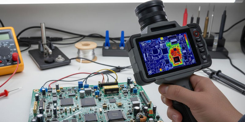
Gerber Files in PCB Manufacturing: Layers, Formats and Checks
Between the design file and the finished board sits a translation step that most engineers treat as a formality. It is not. A Gerber file set is the only description of the board that the fabricator will actually use, and every ambiguity in that set becomes a question, a delay or a board that does not fit. Preparing it properly is part of the design work.
What a Gerber File Contains
A Gerber file describes the geometry of one layer of a board: the shapes, positions and apertures that make up copper conductors, pads, solder mask openings and printed legend. The data is expressed as coordinates and standard apertures rather than as a picture, so it is precise and machine readable.
A complete set therefore consists of several files, one per layer, plus a separate drill file that lists hole positions and diameters with a tool table. Older formats used a second file to describe the apertures, while the modern format embeds that information directly so the output is self-contained.
What Gerber Files Do Not Contain
The format describes physical geometry only. It carries no netlist, no component values and no electrical intent, which means the fabricator cannot tell from the data whether a connection is correct, only whether the shapes match what was drawn. Electrical verification has to happen before the files are generated.
That limitation explains why a board can pass every fabrication check and still be electrically wrong. It also explains why a design rule check and an electrical comparison against the schematic belong to the design stage, not to the data preparation stage where the format can no longer help.
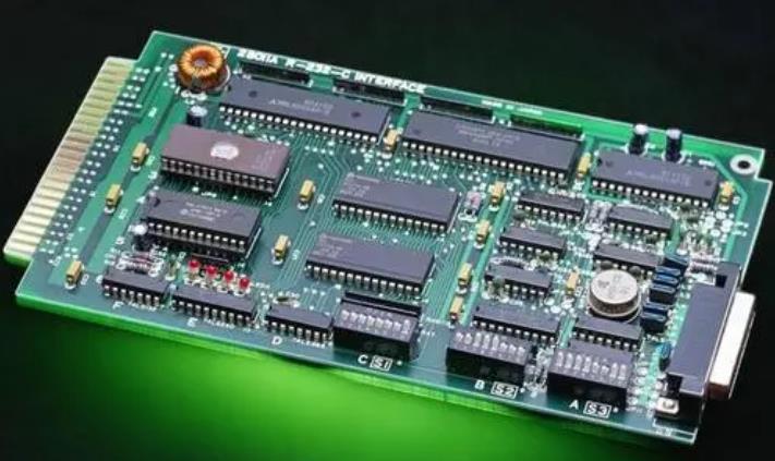
Why the Format Matters
Standardisation is the main advantage. Because the format is universal, a design produced in any tool can be manufactured by any fabricator, and a board developed in one country can be built in another without translation. That portability is worth more than any convenience offered by a proprietary exchange format.
Precision is the second advantage. Coordinates and apertures are stored exactly, so a trace width, a pad size and a hole position are unambiguous. That precision is what allows a four mil trace to be reproduced consistently rather than approximately.
File Types in a Typical Set
A two-layer board typically needs top and bottom copper, top and bottom solder mask, top and bottom silkscreen, the board outline, and the drill file. Inner layers are added for each additional pair, and impedance-critical designs usually include a stackup drawing alongside the data.
Assembly output is a separate matter. Paste layers for the stencil, a component placement file and the bill of materials travel with the assembly order rather than with the bare board order, and they have to agree with the Gerber set about which revision they describe.
RS-274X and Older Formats
The extended format, RS-274X, is the version almost everyone uses today. It includes embedded aperture definitions, which makes each file self-contained and removes the possibility of a mismatch between the layer data and a separate aperture list.
Its predecessor required an accompanying aperture file, and that paired structure is a common source of errors when old data is reused. When a legacy design is reissued, converting it to the extended format and re-running verification is safer than sending the original pair of files.

Generating the Set
Output generation is a repeatable process: complete the layout, run the design rule check, confirm the layer assignments, then export each layer with the correct units and format. Units deserve attention, because a design exported in inches and read as millimetres produces a board one twenty-fifth of the intended size.
Layer naming matters as much as layer content. Names that state both the function and the layer, such as top copper or inner layer two, let a fabricator confirm the stackup without asking. Ambiguous names cost a day of correspondence on almost every order where they appear.
Preparation Checklist
Before export, confirm that the outline is a closed contour with no stray segments, that every drilling requirement is represented in the drill file, that the solder mask openings match the pads they are meant to expose, and that no silkscreen text sits on an exposed pad.
Also confirm the board parameters that the data cannot express: finished thickness, copper weights, surface finish, impedance targets and any tolerance that differs from the standard. Those belong in a short note with the quality characteristics of the design, because they are the items most often assumed rather than specified.
Verifying Before Release
Verification is the step that pays for itself. Open the generated files in a viewer rather than trusting the design tool, compare each layer against its intent, and check the drill file against the via and component hole schedule. Layers that look correct in the CAD window sometimes look very different in the output.
Many fabricators offer a free data check and will report issues such as a missing outline or an unplated hole that should be plated. Taking that offer is worthwhile on any multilayer prototype, since a fault found before the panel is imaged costs nothing, and the same fault found afterwards costs a full fabrication cycle.
The Fabrication Package Around the Data
A Gerber file set is only part of what a fabricator needs. The complete fabrication package also includes the drill file, a stackup drawing with thicknesses and copper weights, the impedance requirements for controlled-impedance nets, the surface finish specification and any tolerance that differs from the standard. Sent together, they describe a board rather than a collection of shapes.
Packaging matters as much as content. A single archive with a clear revision name and a short readme prevents the situation where a stackup note arrives in a later message than the data it describes, and the fabricator builds to the earlier revision. Version confusion is one of the few error classes that no amount of data checking on either side can catch.
It is also worth stating what the package does not include. If paste layers, a placement file and a bill of materials are going to a separate assembly supplier, saying so explicitly stops the bare board fabricator from waiting for files that will never arrive and stops the assembler from assuming the board order includes stencils.
Common Data Errors and How They Show Up
The most frequent problem is a missing or incomplete outline layer, which leaves the fabricator to infer the board edge from the copper. The second is an aperture that was defined in the design tool but never used, which produces a phantom feature in the output that somebody then has to interpret before the panel can be imaged.
A third is a silkscreen that overlaps exposed pads, a cosmetic issue that becomes a solderability question and is usually resolved by deleting the offending reference designators. A fourth is a drill file whose tool table does not match the holes drawn in the copper, which a competent fabricator catches immediately and which produces a day of correspondence on both sides.
All four are preventable with the same habit: open the output in a viewer, layer by layer, and compare what is shown against what was intended. That review takes a few minutes and is the last point at which a mistake costs nothing at all.
FAQ
Can I send the native design file instead of Gerber data? Some fabricators accept it, but the output then depends on their tool version and on how they interpret the file. Exchange data gives you control over exactly what is built.
Is the drill file part of the Gerber set? It is a separate file in a different format, usually Excellon, and it must be sent with the copper layers. A set without a drill file cannot be manufactured.
How do I confirm the stackup is understood? Include a stackup drawing with thicknesses, copper weights and dielectric materials alongside the data. The design and fabrication note is what turns the files into the board you intended.