PCB Lamination: What Happens Inside the Press
PCB lamination is the step where a stack of separate materials becomes one board. Copper foil, prepreg, and cores are bonded under heat and pressure until the resin flows, cures, and locks the layers together. Everything that happens after lamination, from drilling to plating to routing, depends on that bond being complete, and most of the defects that appear later were created or prevented in the press.
What lamination has to achieve
The process has three jobs. It must hold the conductive layers in exact registration, so that pads and vias line up across the stack. It must insulate the layers from one another, because the dielectric strength of the finished board is a property of the cured resin. And it must give the assembly its mechanical strength, so that the board survives handling, component placement, and thermal cycling without delaminating or warping.
A lamination cycle that is too cold leaves the resin under-cured, which shows up as poor dielectric performance and as separation after reflow. A cycle that is too hot or too long degrades the resin, which reduces the same properties from the other direction. The window is defined by the material data sheet and verified by the process, not guessed.
The three materials in the stack
Copper foil provides the conductive layers that carry the signals. Electrolytic foil is the common choice for rigid boards, while rolled and annealed foil is used where the copper has to bend repeatedly, which is a flexible circuit requirement rather than a rigid one.
Prepreg is woven glass impregnated with partially cured resin. It acts as both the adhesive and the dielectric between layers, and its type is chosen from the electrical and thermal requirement: standard FR-4, a high glass transition temperature variant, or a low-loss material for high-frequency work.
Cores are the rigid substrates at the centre of the stack, formed from a base material with copper foil bonded on both sides. FR-4 is the standard, while polyimide and ceramic-filled PTFE appear where temperature or electrical performance demands them.
Preparation and alignment
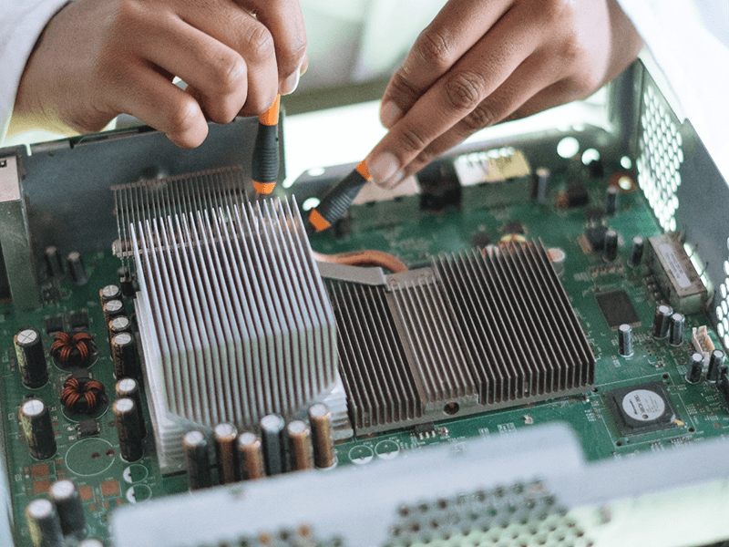
The cycle begins with preparation. Every layer is cleaned to remove contamination that would prevent the resin from bonding, since a fingerprint or an oxide film is enough to create a void. The layers are then aligned using registration holes or tooling pins, which is the operation that decides whether the finished board has pads concentric with their vias.
Registration tolerance is set by the smallest feature in the design. A board with generous annular rings can absorb a small misalignment, while a high-density design with fine lines has almost no margin. That is why the same press can produce acceptable boards for one design and scrap for another.
Alignment is checked before heat is applied, because a stack that shifts during the press cannot be recovered afterwards.
Building the stack
The aligned layers are stacked in the order defined by the design, with prepreg placed between the copper and the cores according to the target dielectric thickness and the required impedance. Layer count is a function of routing density and of the need for reference planes, and multilayer boards commonly run from four layers to more than twenty.
The build should be symmetric where possible. Balanced copper distribution and an even number of layers reduce the internal stress that appears later as bow and twist, and the consequences of ignoring that rule are covered in our guide to balanced stackup and odd layer counts.
The press cycle
Inside the press, the stack is heated while pressure is applied. The resin in the prepreg softens, flows into the spaces around the copper features, and then cures into a rigid dielectric. The important detail is that the flow phase is what fills the gaps: if pressure arrives before the resin is fluid enough, or if the resin is starved in a region with heavy copper, the result is a void or a dry spot that no later process can repair.
Cooling is controlled rather than rushed. A stack that is cooled quickly develops internal stress, because the copper and the dielectric contract at different rates, and that stress is released later as bow, twist, or localised delamination. Gradual cooling under pressure holds the stack flat while it stiffens.
After the press
The laminated panel is trimmed to size, then drilled for through holes, vias, and component mounting. Drilling is followed by plating, which deposits copper inside each hole to connect the layers that the design requires. Those steps are sensitive to the quality of the lamination, because a hole drilled through a void exposes it, and plating chemistry only reaches surfaces that are physically sound.
The finished panel is then processed into its final form: pattern etching, solder mask, surface finish, and test. Everything downstream inherits the registration and the dielectric integrity established in the press, which is why lamination defects are often described as defects that appear somewhere else.
Why lamination quality shows up later
The electrical consequences are direct. Uniform dielectric thickness between a signal layer and its reference plane is what makes controlled impedance possible, and a resin-rich or resin-starved region changes the impedance of every trace that crosses it. Where the laminate is consistent, signal loss and crosstalk behave as predicted, which is what high-speed and high-frequency designs depend on.
The mechanical and thermal consequences are equally direct. Adequate lamination gives the board the strength to survive assembly handling and thermal cycling, and it keeps the structure intact when components heat the board locally. Where the bond is marginal, the board may pass its electrical test and still delaminate after a few reflow cycles.
Advanced lamination techniques
Sequential lamination builds a board in more than one press cycle. Sub-assemblies are laminated first, then combined into the final stack. The technique allows blind and buried vias and tight tolerances to be produced in complex high-density designs, because the inner connections are formed before the outer layers are added.
Low-pressure lamination reduces the cavity risk in thick or complex stacks by applying less force, while vacuum lamination places the stack in a vacuum bag so that air is removed and pressure is distributed evenly. Both techniques address the same problem, which is trapped air and uneven resin flow in a stack that has little room for error.
Advanced lamination is a capability question rather than a specification question. A stack that requires three press cycles should be quoted by a shop that runs them routinely.
Quality control on the laminated panel
Inspection starts visually. Voids, delamination, and misalignment are checked under magnification, and automated optical inspection is used where the volume justifies it. Electrical test then verifies the connections: continuity between points that must be joined, insulation resistance between points that must not, and impedance on controlled nets.
Thermal testing closes the loop. Thermal cycling and thermal shock expose marginal bonds by forcing the copper and the dielectric to expand and contract at different rates, and thermal imaging locates the spots that heat up faster than they should. A board that survives those tests has demonstrated the property that lamination exists to provide. How the stack itself is planned around reference planes is covered in our guide to layer stackup from one to eight layers, and the dimensional effects of a poor press cycle are described under PCB dimensional stability and expansion.
FAQ
How long does a lamination cycle take? The press time runs from roughly an hour to several hours depending on the material, the stack thickness, and the profile. The cooling phase is part of the cycle and should not be shortened to save time.
What causes delamination? Moisture in the prepreg, contamination on a copper surface, an incomplete cure, and rapid cooling are the usual causes. All four are process conditions rather than material defects.
Can a laminated board be repaired if a layer separates? Not reliably. Once the resin has cured and the bond has failed locally, the repair cannot restore the dielectric in that area, so the panel is normally scrapped.