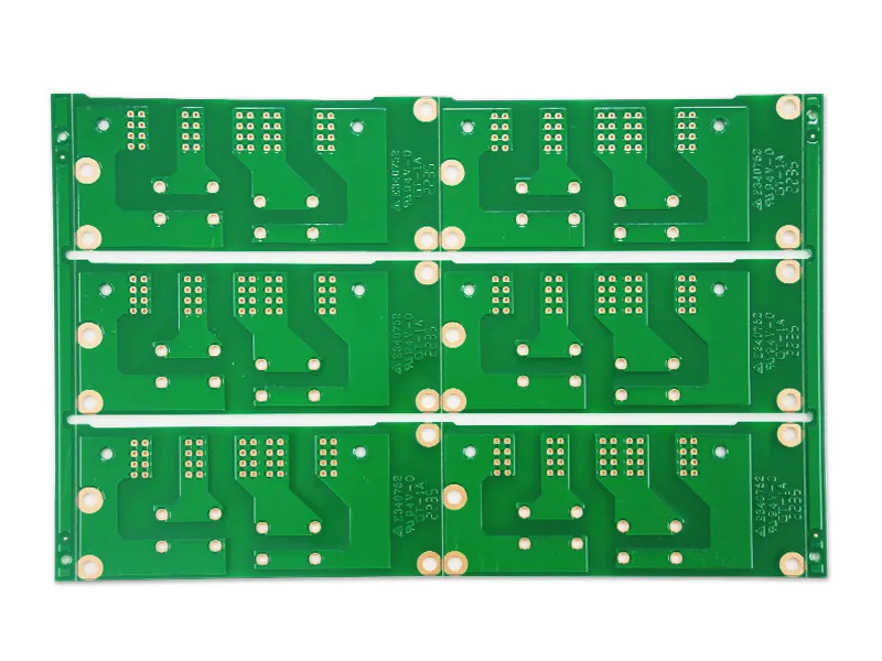
Stepped Rigid-Flex Board: Design Guide for Cavity and Step Structures
A stepped rigid-flex board changes thickness across the same outline. A rigid section may be four layers thick, the flex section two, and the components may sit in a cavity milled into the structure so that total height stays within a mechanical envelope. The shape is familiar from camera modules, wearables and medical probes.
The step is a mechanical feature that the fabrication process must create, and every step constrains the layout around it. Understanding where those constraints fall is the difference between a manufacturable design and one that generates concessions on the first order.
Why Steps and Cavities Are Used
Three requirements drive the structure. The first is height: a component that is taller than the available space must sit in a cavity so that the assembly fits the enclosure. The second is bending: the flex region must be thin enough to bend to the required radius while the rigid region stays stiff enough to carry components.
The third is electrical. In high-frequency designs, a controlled step can keep the distance between a component and a reference plane constant across a section that would otherwise change thickness, which keeps impedance predictable.
<img src="https://www.gopcba.com/wp-content/uploads/2026/02/PCB-Assembly.png" alt="Stepped rigid-flex board with cavity and flexible bend area” />
Cavity Depth and Tolerance
Cavity depth is controlled by depth milling, laser ablation or a controlled lamination build-up, and each method has a different tolerance. Depth milling removes material from a specific area of the finished board and depends on precise depth control, because the process must stop at a target layer without cutting through it.
Designers should specify the cavity as a target with a tolerance band on both depth and position, and state which layer must remain intact beneath it. Without that statement, the fabricator has no way to know how much margin the design can accept.
The cavity edge also needs attention. A sharp internal corner concentrates stress, so cavities are usually drawn with radiused corners, and the copper beneath should avoid the boundary region.
Layer Transitions and Bend Areas
A layer transition is the point where the stackup changes from rigid to flex. It carries the highest mechanical and thermal stress on the board: the rigid material and the polyimide flex expand differently, and bending forces concentrate at the boundary.
Design the transition so that vias and traces stay clear of the boundary region, and route the conductors that cross it perpendicular to the edge rather than parallel. A trace that runs along the transition edge experiences the largest strain and is the first to crack.
The bend area must be free of plated through-holes, stiffeners and coverlay openings. It should also be designed with a defined bend radius in mind, since a dynamic bend, repeated many times in service, requires a larger radius and thinner construction than a static bend that is formed once during assembly.

Stiffener Placement
A stiffener is bonded to the flex area to create local rigidity for connectors, component placement or a press-fit feature. Its material, thickness and position must be documented, and its edge must never fall inside a bend area.
Stiffeners also affect assembly. A component placed on a stiffened section sits higher than one on bare flex, so the placement program must account for the change in height. Where the stiffener is added after reflow, the assembly sequence has to be stated explicitly.
Cavity Assembly Considerations
Components placed in a cavity are harder to assemble and harder to inspect. Paste printing requires the stencil to be supported so that it does not sag into the cavity, and a step stencil or a dedicated carrier may be needed.
Optical inspection is affected as well, because access and lighting change inside a recess. Where a cavity contains hidden joints, X-ray inspection is usually required, and the test plan should say so rather than leave it to be discovered during production.
Fabrication Limits to Respect
Fabricators publish limits for minimum cavity size, aspect ratio of the milled depth, minimum flex thickness and maximum number of lamination cycles. These limits are process-specific, and designs that exceed them require tooling development rather than a price negotiation.
Sequential lamination adds another dimension: a stepped board with buried vias may need several press cycles, and each cycle adds registration risk. Keeping the step structure as simple as the mechanical requirement allows reduces the number of cycles and the cost.
Documentation for a Stepped Design
The fabrication drawing for a stepped rigid-flex board needs more information than a standard board. It should state the stackup for each zone, the cavity depth with tolerance and the layer that must remain, the bend radius and whether the bend is static or dynamic, and the stiffener material and location.
A cross-section drawing is worth more than a page of notes. It shows the zones, the transitions and the interfaces in one view, and it removes the ambiguity that produces questions after the order is placed.
Cost and Lead Time Drivers
A stepped rigid-flex board costs more than a plain rigid board of the same size, and most of the difference comes from processing cycles rather than from material. Each additional lamination, each depth milling operation and each cavity adds handling between steps.
Lead time follows the same pattern. Cavity milling and stiffener bonding are usually the operations that determine the schedule, because they are performed by specific equipment that may run on a separate line from the rigid board process.
Where the mechanical requirement is flexible, simplifying the structure pays directly. Replacing a cavity with a lower-profile component or moving a stiffener away from a transition can remove an entire process step without changing the electrical function of the board.
Verification and Test
Verification follows the mechanical intent. Assembled samples are bent to the specified radius for the specified number of cycles, thermally cycled between the service extremes, and inspected for continuity across the transitions.
Microsectioning at the transition and at the cavity edge reveals whether plating survived the bending and the lamination cycles. That single destructive check explains most of the failures that otherwise appear as intermittent opens in the field.
Mechanically, the cavity also removes material that would otherwise stiffen the board, so the outline around it usually needs additional support or a localized stiffener to keep the assembly flat during handling.
Related reading: multilayer prototype requirements, via in pad versus plated through, and board outline and mounting design.
Treat the step structure as a mechanical requirement to be reviewed alongside the enclosure model, not as a layout detail to be resolved at the end. Most stepped designs that fail do so because the cavity was drawn after the components were placed.
FAQ
Can a cavity be added to an existing design? Only with a new fabrication cycle that includes additional tooling. The cavity changes the stackup and the layer structure, so it is a design revision rather than a process option.
What is the minimum achievable cavity depth? It depends on the process and the number of layers removed. Depth milling and laser ablation reach different limits, so the requirement should be discussed with the fabricator against the specific stackup.
Is X-ray necessary for a stepped board? For any joint that is hidden inside a cavity or under a package, yes. Optical inspection cannot reach those joints reliably, and the cost of X-ray is small compared with a returned assembly.