PCB Copper Weight: 1 oz, 2 oz and 3 oz Compared
PCB copper weight is one of the few board specifications that affects electrical performance, thermal behaviour, mechanical durability and price at the same time. It is also frequently specified by habit rather than by calculation, which is why some designs pay for copper they do not need while others cook a power device that would have been fine with a heavier layer.
What Copper Weight Means
Copper weight describes the thickness of the foil or plated copper on a layer, expressed as the weight of copper spread over one square foot. One ounce per square foot corresponds to roughly 35 microns of copper. Two ounces is about 70 microns, and three ounces about 105 microns.
The unit is historical, but the meaning is simple: doubling the weight roughly doubles the cross-sectional area of a trace of the same width, which halves its resistance per unit length and increases the current it can carry.
Thickness, Weight and Area
Converting between units is a useful sanity check. Copper has a density of about 8.96 grams per cubic centimetre, so a square inch of one ounce copper weighs roughly 1.25 grams, two ounce copper about 2.5 grams and three ounce copper about 3.75 grams. Those figures describe the copper itself, not the finished board.
The finished weight of a board depends on the laminate, the number of layers, the surface finish and the components when it is assembled. Copper weight is therefore an input to the calculation rather than the answer to it.
Current Capacity and Voltage Drop
The current a trace can carry is limited by the temperature rise it is allowed to produce. A wider trace or a thicker layer both reduce resistance, and the two are interchangeable to a first approximation: doubling the copper weight has a similar effect on resistance to doubling the trace width.
Width is usually the cheaper lever, because it costs only board area, while heavy copper costs material and process time. Where area is scarce, weight becomes the practical answer. The calculation should be performed with the trace width and current calculation for the specific temperature rise the product allows.
<img src="https://www.gopcba.com/wp-content/uploads/2025/08/21.png" alt="PCB cross section showing copper thickness on inner and outer layers” />
Thermal Spreading Under Power Devices
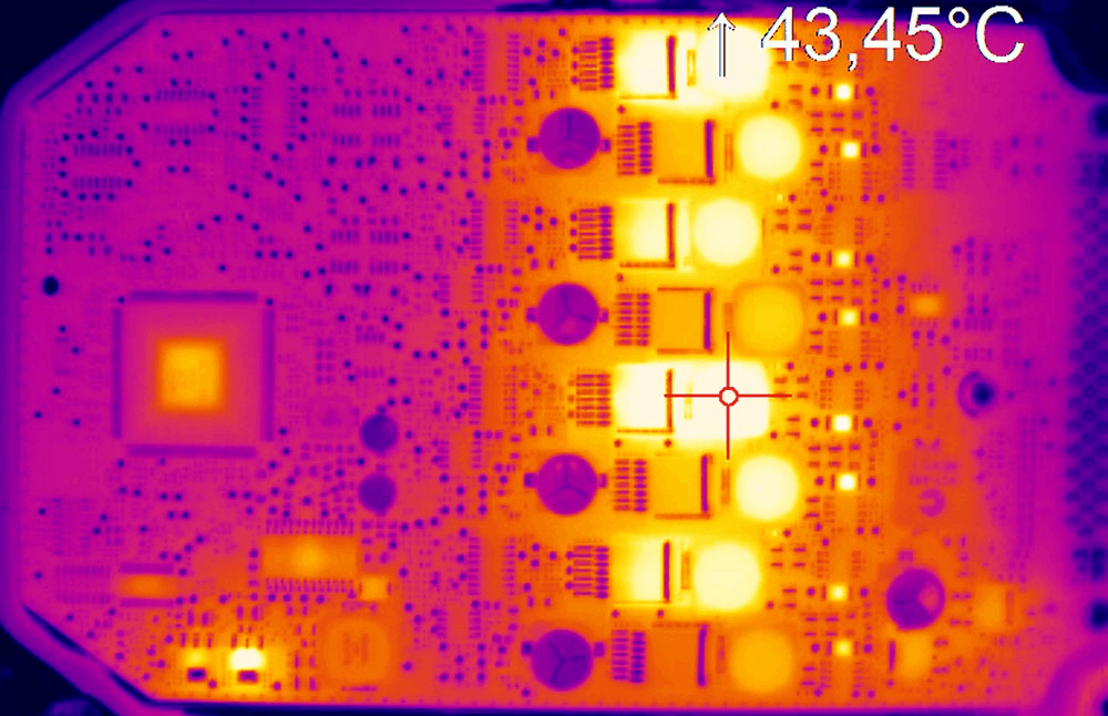
Copper weight matters as much thermally as electrically. A power device soldered to a pad transfers heat into the copper beneath it, and the spreading resistance of that copper determines the temperature drop between the device and the wider plane or heat sink.
Two ounce copper spreads heat noticeably better than one ounce, and heavy copper spreads it better still, which is why LED drivers, motor controllers and power supplies often specify 2 oz or more even when the current alone would not require it. Techniques such as copper flooding complement the heavier layer by increasing the effective area.
Etching Limits and Minimum Trace Width
Heavier copper is harder to etch. The etchant attacks sideways as well as downwards, so a thick layer produces more undercut and a trapezoidal cross section. The practical consequence is a larger minimum trace width and spacing for a given process.
On 2 oz copper, a fabricator may hold 6 to 8 mil lines comfortably, while 3 oz pushes the minimum higher and makes fine-pitch routing difficult. Designs that combine heavy copper with dense componentry usually need the power layer to be heavy and the signal layers to stay at 1 oz.
Layer Count, Weight and Lamination
Heavy copper affects lamination. Thick traces create topography that the prepreg must fill, and insufficient resin flow leaves voids or resin starvation around the conductors. The fabricator compensates with additional prepreg or a planarising step, both of which add cost.
Copper balance also becomes more critical. An inner layer with large heavy-copper pours adjacent to a sparse signal layer can laminate unevenly, and the resulting thickness variation distorts impedance on any controlled-impedance layer in the same stackup.
Choosing 1 oz, 2 oz or 3 oz
One ounce remains the default for signal layers and for low-power digital products, because it is the cheapest, the easiest to etch and entirely adequate for logic currents measured in milliamps.
Two ounce copper suits products that combine moderate current with a thermal requirement: LED lighting, motor drivers, power conversion stages and automotive modules. It is the usual compromise between capacity and cost.
Three ounce copper and above appear in power supplies, high-current distribution, inverter stages and applications that must survive surges. Above that, heavy copper becomes a specialized process, with planar copper up to 20 oz available for bus bars and high-current assemblies.
Heavy Copper Above 3 oz
Heavy copper fabrication uses thicker starting foils, longer etch cycles and often a filled and planarised construction so that subsequent layers can be laminated flat. Some processes use additive techniques to build up thick conductors where they are needed rather than etching them from a heavy foil.
The electrical benefit is significant: a 6 oz trace carries several times the current of a 1 oz trace of the same width, and it also conducts heat into the board structure far more effectively. The cost is a much narrower process window.
Specifying Copper Weight Correctly
State the weight for each layer rather than for the board as a whole, and confirm whether the value refers to the starting foil or to the finished copper including plating. On outer layers, plating adds to the finished thickness, so a 1 oz base becomes roughly 1.5 oz after a standard plate, and impedance calculations must use the finished value.
Then check the design against the process. Confirm the minimum trace width and spacing for the chosen weight, verify that the prepreg can fill the topography, and review the power distribution with ground and power trace planning so the heavier layer is used where it actually helps. Where heavy copper is combined with dense vias, review copper plating defect prevention before release.
Copper Weight and Surface Finish Interaction
Heavy copper and surface finish choices interact in ways that are easy to overlook. A hot air solder leveling finish on thick copper produces a more uneven surface, because the solder volume on a heavy pad is larger and the leveling air cannot flatten it as effectively. On fine-pitch parts over heavy copper, that unevenness affects paste release.
Planar finishes such as electroless nickel immersion gold avoid the problem but add cost, and the nickel layer becomes the limiting factor for the joint rather than the copper beneath it. The practical rule is to keep heavy copper away from fine-pitch assembly areas and specify the finish for the assembly process rather than for the power requirement.
It is also worth confirming how the fabricator reports copper weight on the finished board. Plating adds thickness on the outer layers, so the value in the impedance model has to be the completed copper thickness rather than the foil the panel started with.
FAQ
Is heavy copper needed for a 10 A trace? Not necessarily. A wide 1 oz trace can carry substantial current if the board area allows it. Heavy copper becomes the answer when width is constrained or when thermal spreading is also required.
Does copper weight affect impedance? Yes, because it changes the thickness of the conductor and therefore its resistance and, to a lesser degree, its inductance. On controlled-impedance layers the finished copper thickness must be used in the calculation.
Can fine-pitch parts be used with 3 oz copper? Usually only on the power layers. Fine-pitch devices need narrow traces and small pads, and those features are difficult to hold reliably on heavy copper. Splitting the stackup so that signal layers remain light is the standard solution.