BMS PCB Design: Layout Rules for Battery Management Systems
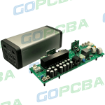
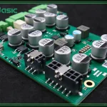
A BMS PCB is the board that measures, protects and balances a battery pack. It combines a high-current path, a precision measurement chain and a control section, and the three have very different layout requirements.
Almost every design problem on a battery management board comes from mixing those three domains. The layout must keep the current path out of the measurement, and the measurement out of the switching noise of the control circuits.
What a BMS Board Does
The board measures cell voltages and pack current, protects the pack against over-charge, over-discharge, over-current and over-temperature, balances the cells so that they age evenly, and communicates state to the host system.
Each function has its own accuracy requirement. Cell voltage measurement typically needs millivolt accuracy, current measurement may need better than one percent across a wide dynamic range, and the protection thresholds must not drift with temperature.
High-Current Path Layout
The main current path carries amps to hundreds of amps and should be treated as a mechanical and thermal design problem, not only an electrical one. Copper weight, trace or busbar cross section, and the number of parallel vias all determine how much heat is generated.
Copper thickness is the usual answer. Two to four ounce copper, or a soldered busbar, keeps voltage drop and temperature rise manageable. Where a trace changes layers, use many vias in a matrix rather than a few large ones, because current distributes according to resistance.
Keep the main current path short and direct. Every extra millimetre of copper adds resistance and heat, and any loop formed by the layout becomes a source of magnetic coupling into the measurement circuits.

Shunt Resistor and Current Sensing
The shunt resistor converts current into a small voltage. Its layout determines the accuracy of the entire current measurement, because the sense connections must tap the resistive element exactly where the manufacturer specifies.
Sense traces are routed as a differential pair to the measurement amplifier, taken from inside the shunt terminals, and never from the copper that carries the load current. Routing the sense connection outside the shunt means the measured voltage includes the drop in the connecting copper.
Kelvin connections are the standard. The sense pair should be symmetric, equal in length and kept away from the high-current path, and they should cross no plane split. Temperature compensation matters too, so the sense resistor should not be placed next to a heat source.
Isolation and Creepage
Where the control electronics share a board with a high-voltage pack, isolation is mandatory. The isolation barrier separates the measurement side from the communication side, and its physical layout is governed by creepage and clearance distances rather than by component ratings alone.
Creepage is the distance along the board surface, and it depends on the pollution degree and the material group of the laminate. Clearance is the distance through air, and it depends on the working voltage and the altitude at which the product operates.
Design rules follow: keep the barrier free of copper, provide slots where the required creepage cannot be achieved on the surface, and route no signal across the barrier except through the isolated device that is intended to cross it.
Cell Balancing Circuits
Cell balancing circuits are repetitive, and their layout should be equally repetitive. Each balancing channel needs its own resistor, switch or transistor and connection to the adjacent cell, and any asymmetry between channels produces uneven balancing behavior.
Balancing resistors dissipate real power, and they are usually the hottest components on the board. Spreading them rather than grouping them distributes heat, and keeping them away from the monitoring device prevents the thermal drift of the measurement.
Measurement Accuracy
Accuracy depends on the reference, the amplifier and the layout. A shared reference with a stable temperature coefficient is the starting point, and the reference should be placed away from switching regulators and balancing resistors.
Grounding determines what the measurement actually sees. The analog measurement ground should be separate from the power ground and joined at one point, usually beneath the monitoring device, so that the large currents in the power path do not create voltage differences in the measurement reference.
Thermal Management
Power dissipation in a BMS board comes mainly from the main current path, the balancing resistors and the protection switches. Each needs a thermal path to copper area or to the enclosure.
Thermal vias under power devices, wide copper pours and a mounting design that couples heat into the chassis are the basic tools. Where the pack is sealed, conduction is the only path available and the copper becomes the heatsink.
Communication and Control Section
The communication interface, whether CAN, SPI or a wireless link, belongs on the isolated side of the board. Its routing should avoid the current path and the switching regulators, and the transceiver should have its own decoupling close to its pins.
Where a microcontroller shares the board with switching circuits, keep its ground and supply clean. A marginal supply shows up as communication errors that correlate with load current rather than as an obvious reset.
Protection and Fault Behaviour
The protection switches must be able to interrupt the maximum fault current without exceeding their safe operating area, and the layout determines how quickly they can respond. Gate or base drive traces should be short and return to the driver by a defined path.
Where a fuse or a contactor shares the board, its position defines the order in which the pack is disconnected, and the layout should reflect the intended sequence so that no component sees an over-voltage during a fault.
Connector and Mechanical Design
High-current connectors carry mechanical load as well as current. Their pads need enough copper and enough vias to distribute the current, and the enclosure should support the connector so that cable force is not transmitted into the laminate.
Mounting points are part of the thermal design. A BMS board bolted to a metal housing conducts heat out through the mounting hardware, which is often the most effective thermal path in a sealed pack.
Design Checklist
Confirm the current path cross section against the maximum current and the allowed temperature rise, verify the shunt sense routing against the manufacturer recommendation, check that creepage and clearance meet the applicable standard, and place the balancing resistors so that their heat does not reach the measurement components.
Then verify the isolation barrier on the finished layout, not on the schematic. The barrier is a physical feature, and a design that meets the requirement on paper but has a via or a plane crossing it does not meet it in practice.
Related reading: trace width and current calculation, ground routing and power trace planning, and DC-DC converter layout and routing.
FAQ
Why does my current measurement drift with load? Usually because the sense connection is taken outside the shunt element or the sense pair runs parallel to the high-current path. Both make the measurement include copper resistance that changes with temperature.
How much copper is needed for a high-current path? Enough to keep voltage drop and temperature rise inside the design limits, calculated from the current, the copper thickness and the available area. Busbars are used where copper alone is insufficient.
Can a BMS board be non-isolated? For low-voltage packs, yes. Above the safety threshold defined by the applicable standard, an isolation barrier with verified creepage and clearance is required.