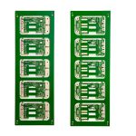
Metallized PCB Edge: Edge Plating and Castellation Design
A metallized PCB edge carries copper onto the side wall of the board, either as a continuous plated band or as a row of castellated half holes. The first is used mainly for shielding, grounding and current return; the second turns a small module into a surface mountable part with solderable edge pads. Both change the way the panel is routed, drilled and plated, so they have to be designed before the outline is finalised.
Edge Plating and What It Does
Edge plating connects the top and bottom copper of a board around its perimeter. For a product with a metal enclosure, it provides a low impedance path from the ground plane to the chassis, which is one of the most effective ways to control radiated emissions. It also routes return currents around the edge of the board instead of forcing them through a narrow internal layer.
The plating can be continuous around the whole outline or limited to selected segments, and it can be tied to a specific net such as chassis ground. Where isolation is required, the plated band is left unconnected or separated by a routed slot.
Castellations and Half Holes
A castellation is a plated through hole that is cut in half by the board outline, leaving a copper lined notch on the edge. A module built this way can be soldered onto a carrier board like any surface mount component, which removes the need for a connector and reduces height. The same feature is used on small radio modules, sensor packages and power bricks.
The half hole has to be drilled and plated as a full hole first, then the final routing cuts through the centre. That means the hole position must be known exactly at the drilling stage, and the router must follow the plated pattern without leaving burrs or smearing the copper.
Fabrication Limits and Tolerance
Castellation diameter is normally 0.6 mm or larger for reliable plating, with a finished tolerance of about ±0.05 mm. Smaller holes can be produced, but the plating in a half barrel becomes difficult to control and the mechanical strength of the notch falls.
The rout path should pass through the hole centre within about 0.05 mm, because an offset leaves one side of the notch thicker than the other and produces an uneven solder fillet. Spacing between adjacent castellations is usually at least 0.5 mm to leave web material that can survive handling, and the edge copper should be kept clear of the final route by enough margin to prevent burrs and delamination.
Soldering and Wicking Control
Solder wicking is the main assembly risk. The plated barrel is open on the outside, so molten solder can travel up the notch and into the module if the paste volume is too high or the reflow profile is too long. Aperture design should therefore print slightly less paste than for a normal pad of the same area.
Some designs add a small solder mask dam at the top of the notch to limit wicking, and others rely on a controlled reflow profile with a shorter time above liquidus. The topic is closely related to the finish discussion in the comparison of lead-free and leaded solder, because a higher melting point alloy reduces the time available for wicking at the same peak temperature.
Layout Rules Around the Outline
Copper near the board edge must be pulled back from the rout path on standard boards, but that rule is inverted for edge plating: the copper has to reach the edge and be exposed on the wall. The internal clearance should be stated on the drawing for each segment, along with the layer on which the band runs.
Slots, cutouts and internal routing have to be planned together with the plating, because a routed slot crossing a plated edge breaks the electrical path. The interaction between slots and nearby traces is described in the notes on slot and edge routing rules, and the mounting constraints are covered in the guidance on board outline and mounting design.
Designing the Outline Drawing
The mechanical drawing is the single most important document for this type of board. It should show the outline, the plated segments, the castellated positions, the slot geometry and the tolerances for each. Ambiguity between the Gerber outline and the drawing is the usual reason a delivered board has plating in the wrong place.
Specify the copper weight on the plated edge, the finish applied to it and whether the band is connected to ground or left isolated. If the edge will be used as a wear surface for a connector, hard gold should be specified rather than a thin immersion finish, because repeated insertion will erode a soft layer quickly.
Applications
Edge plating appears in shielded instrument enclosures, RF modules, automotive control units and industrial products that must pass emission limits. Castellations dominate in modules: radio transceivers, sensor nodes, power converters and any design where a carrier board plus a daughter module is cheaper than a larger single board.
Cleaning, Coating and Reliability
An exposed copper edge is more vulnerable than the rest of the board. The plated band is not covered by solder mask, so it can oxidise, collect contamination and, in a humid environment, provide a leakage path along the side wall. Cleaning before coating is therefore more important here than on a standard assembly, and the cleaning chemistry has to be compatible with the finish on the edge.
A conformal coating applied over the assembled board will not protect the edge if the plated band has to remain exposed for grounding. Where the edge is a wear surface or a contact area, a harder finish is specified instead, and the rest of the board is coated around it. The general approach to protecting a finished assembly is described in the notes on conformal coating as board protection.
Testing and Quality Control
Verification of a plated edge starts with a visual check for plating coverage, burrs and delamination, and continues with a continuity measurement between the edge band and the ground plane it is meant to serve. A band that looks complete but has a thin or broken connection passes inspection and fails in the field.
Castellated holes are checked for barrel coverage and for the position of the rout relative to the hole centre, usually by cross sectioning a sample module. Insertion and pull-off tests on a soldered module confirm that the notch geometry gives the expected joint strength. If the modules are to be soldered by the customer, a sample reflow with the recommended profile should be run before the design is released.
FAQ
Is edge plating the same as a castellated edge? No. Edge plating is a continuous band along the side wall, while castellations are individual half holes on the outline. Some boards use both, with a plated band between castellated pads.
Does edge plating improve EMC? It gives the ground plane a direct, low impedance connection to the enclosure, which reduces emissions and improves immunity. The benefit depends on how well the enclosure and the plated segments are bonded together.
Can castellations be added to an existing layout? They can, but the holes must be placed before fabrication and the outline routed through them. Adding them after the panel has been drilled is not possible.