PCB Etching: Process Control, Tolerance and Cost Factors
PCB etching removes the copper that the resist does not protect, and it is the step that determines whether the trace widths on the finished board match the widths in the design. Because the process removes copper in every direction, a nominal trace always arrives smaller at the top than at the base.
Etching is also one of the least expensive steps to control and one of the most expensive to get wrong. A drifting etch line produces shorts and opens across an entire panel, so the process is monitored continuously rather than inspected at the end.
Subtractive and Additive Processes
The traditional process is subtractive: copper is laminated over the whole panel, the pattern is defined by resist, and the unwanted copper is dissolved away. It is simple and inexpensive and it is used for the majority of boards.
Semi-additive processing works the other way: a thin seed layer is patterned, copper is plated up only where conductors are required, and the seed is removed. It achieves finer lines because there is no lateral etching of the conductor.
Which process is used is determined by the required line width. Below roughly 50 microns, subtractive etching becomes impractical and a semi-additive route is required, which is one reason fine-line boards cost more.
The Etch Factor and Undercut
The etch factor describes how far the etchant removes copper sideways relative to the depth removed. In a standard process, a trace with a trapezoidal cross section results, and the top width is narrower than the base width by roughly twice the etch depth times the etch factor.
Undercut is the same effect seen from the resist side. If the resist adhesion is poor, the etchant can penetrate beneath the resist edge and remove copper that should have been protected, and a trace that was designed at the minimum width becomes a reliability risk.
Thicker copper makes both effects worse. Removing a two ounce layer takes longer, and the lateral removal accumulates over that time, which is why heavy copper boards have larger minimum feature sizes.
Uniformity Across the Panel
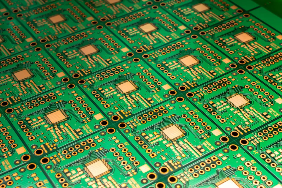
Etch rate depends on the local copper density, the spray pressure and the position of the panel in the conveyor. Areas with little copper etch faster than dense areas, and the middle of a panel behaves differently from the edges.
Fabricators compensate by adjusting the artwork so that the finished trace lands near its nominal width, and by controlling spray uniformity and conveyor speed. The compensation is developed per process and per copper weight rather than transferred from one line to another.
The result is a trace width tolerance, which designers must respect. A design drawn at the process minimum has no margin for the narrow end of that band.
Common Etch Defects
Shorts occur where the etchant failed to clear copper between two conductors, usually because of insufficient spray, a resist defect or a copper sliver that was not removed. They are detectable by electrical test but not always by visual inspection.
Opens occur where a conductor was partially or fully removed, typically from over-etching, resist lifting or a scratch in the resist. Opens in a fine line are often marginal rather than complete, which makes them the more dangerous failure because they pass test and fail later.
Residual copper and chemical staining are cosmetic in some cases and functional in others. A residue between two conductors is a potential leakage path, especially where the board will be exposed to humidity.
Achieving Etch Process Uniformity
Etch process uniformity is the property that makes a panel predictable: the same feature receives the same amount of etching wherever it sits on the panel. Without it, a design that works in the centre of a panel fails at the edge.
Uniformity is produced by balancing spray pressure and nozzle condition, controlling conveyor speed and etchant temperature, and managing the dissolved copper level in the bath. Dense and sparse areas on the same panel are the hardest case.
Where a design has large copper areas next to fine features, a hatched copper pattern and a uniform distribution of traces reduce the imbalance. That is a design contribution to process uniformity, and it costs nothing to include.
Process Control and Measurement
Etching is controlled with a combination of bath analysis and panel measurement. Etchant concentration, temperature and the dissolved copper level are monitored, and coupons on the panel are measured to verify the resulting trace width.
The measured width feeds back into the artwork compensation. A process that drifts is corrected by adjusting the chemistry or the conveyor speed rather than by changing the artwork for every panel, because the artwork is a fixed tool.
Design Rules That Follow
Work one increment above the process minimum for trace width and gap. That single rule removes a large share of yield loss at negligible cost in board area.
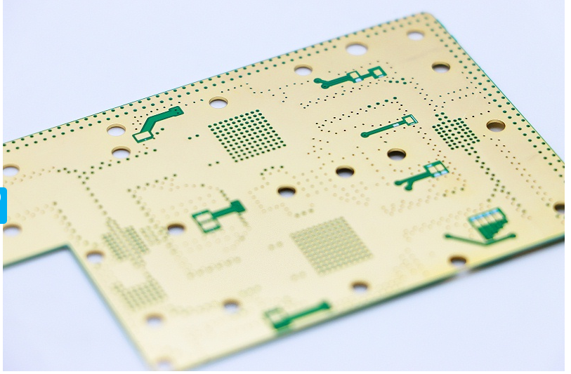
Keep copper distribution reasonably uniform across the panel, and avoid large isolated areas that etch at a different rate from their surroundings. Where a large copper area is required, a hatched pattern etches more uniformly than a solid one.
Provide adequate spacing between features so that the etchant can circulate and the resist can adhere. Very tight gaps are achievable, but they reduce the process window and increase the cost of every panel in the lot.
Etch Process and Cost
Etching cost is dominated by the chemistry, the energy used for the conveyor and pumps, and the waste treatment of the spent etchant. Those costs are largely fixed per panel, so etch cost is not sensitive to the pattern unless the pattern requires a tighter tolerance.
A pattern that requires tighter tolerance costs more because it reduces yield and requires more inspection, not because the etchant itself is more expensive. That distinction is useful when reviewing a quotation: the price difference comes from control and inspection, not from materials.
Inspection and Acceptance
Acceptance is based on measured coupon values, electrical test, and visual criteria for residues and staining. Where fine lines are used, automated optical inspection supplements the electrical test that cannot detect a marginal conductor.
For high-reliability boards, microsections may be used to verify the trace profile at the customer’s request. That is an added cost item, and it should be specified only where the trace geometry is critical to the electrical performance.
Coupons and Verification
Coupon structures on the production panel carry test traces at the minimum designed width, so the etch result can be measured without sectioning a board. The measured value is compared with the design and with the tolerance band, and the difference feeds back into the artwork compensation.
Where impedance-controlled nets are present, the same coupon provides the impedance measurement, so the etch verification and the impedance verification can be performed on the same structure.
Design Checklist
Check the minimum trace and gap against the fabricator capability for the copper weight being used, confirm the tolerance band on critical features, and review the copper distribution for uniformity.
For impedance-controlled lines, remember that etch tolerance translates directly into impedance tolerance. The two should be specified together, and the fabricator should be told which nets are affected.
Related reading: PCB manufacturing tolerances, PCB manufacturing processes, and copper plating defect prevention.
FAQ
Why is my trace narrower than the design? Because etching removes copper laterally as well as in depth. The top of the trace is always narrower than the base, and the fabricator compensates with artwork adjustment.
Can heavy copper be etched to fine geometry? Not efficiently. Thicker copper requires longer etching, which increases lateral removal, so minimum feature sizes are larger on heavy copper layers.
What causes a trace to open after passing test? A marginal conductor that was partially thinned during etching. It often measures acceptable at test but fails under thermal cycling or mechanical stress.