IC Package Types: From DIP to BGA and CSP
Every integrated circuit reaches a circuit board through a package, and the package is often chosen long before anyone thinks about soldering it. That is a mistake, because the package sets what the board has to tolerate: how many pins must escape a shrinking footprint, how much heat has to leave the die, how much inductance sits between the die and the board, and how tightly the assembly process has to be controlled. Understanding the family of IC package types and what each one trades away makes the choice much easier.
What a Package Has to Do
Four jobs. It has to protect the die from the environment, providing a barrier against moisture, contamination, and mechanical damage. It has to fan the die connections out to a lead pitch the board can handle. It has to provide a thermal path from the die to the board or to a heatsink. And it has to be manufacturable at the required volume at an acceptable cost.
The package also carries an electrical cost. Every millimetre of lead adds inductance and capacitance, and every connection adds a small resistance. A package that is mechanically convenient but electrically long will limit bandwidth regardless of how good the die is.
The Ratio That Predicts Everything
The single most useful measure of a package is the die-to-package ratio, the silicon area divided by the package footprint. A ratio close to one means the package adds very little area beyond the die, which is the direction the industry has moved for decades. A low ratio means the board carries considerably more footprint than silicon, which costs board area, routing room, and, in volume, money.
The Through-Hole Era: TO and DIP
The earliest packages were metal cans and dual in-line packages. A DIP has two rows of leads on a 2.54 mm pitch and is inserted through holes in the board. Its advantages are mechanical robustness and easy hand assembly; its disadvantage is the area it consumes, since each lead needs a hole with a solder joint and a keep-out around it.
Surface Mount Arrives: PLCC, QFP and Its Thin Variants
Surface mount removed the holes and let the leads sit on pads. PLCC placed leads on all four sides in a J shape; QFP flattened them into a gull-wing. The quad flat family then split into thin variants for low profile and plastic variants for volume, and the pin pitch dropped from about 1 mm to 0.65, 0.5, 0.4 and eventually 0.2 mm.
A large quad flat package can place well over a hundred leads on a side, and that is where the design problem starts. At 0.5 mm pitch, escape routing from the inner pins needs vias between pads, which pushes the board toward finer lines and additional layers. These parts also carry longer leads than ball-grid equivalents, and lead inductance is what limits their use in the fastest interfaces. They remain common in microcontrollers and medium-density logic, where their repairability and their visible joints are genuine advantages.

Thin Small Outline and Memory
For memory, the thin small outline package was the standard for years: leads on two sides, low profile, inexpensive, and suited to surface-mount assembly. It is limited by the inductance of its leads, which is why high-speed memory moved on when bandwidth requirements grew.
Ball Grid Array
A BGA replaces the leads with an array of solder balls on the underside. The important consequence is that the same number of connections can be arranged on a coarser pitch, because they use the area of the package rather than its perimeter. Assembly yield improves, and inductance drops because each ball is short and the connection is direct. The die-to-package ratio improves as well.
The trade-off is inspectability. The balls are underneath the package, so optical inspection cannot see the joints, and X-ray becomes mandatory for verifying them. Repair is harder, requiring reflow of the whole array rather than an iron on a pin. BGAs also require careful attention to package warpage and to the reflow profile, since a warped package and an uneven ball array produce opens that routine inspection may not catch.
Chip scale packages take the same idea further and approach a die-to-package ratio of one, which is where the smallest portable products now live.
What the Package Forces on the Board
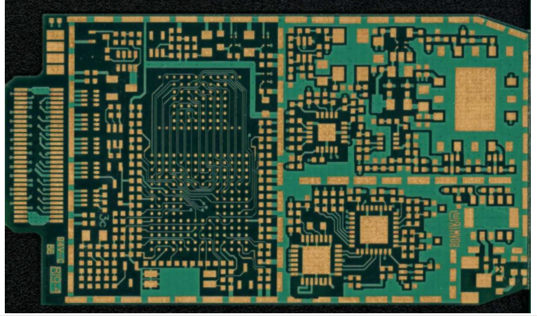
The package choice propagates into the layout. A fine-pitch perimeter package needs escape routing and often via-in-pad structures, which drives layer count and process complexity. A ball-grid array needs controlled-impedance breakouts, thermal vias for heat removal, and X-ray inspection at assembly. A thin package with a large exposed pad needs a stencil aperture and reflow profile tuned so that the pad does not starve the surrounding joints of paste.
Placement and pad geometry follow the package as well: the pad design has to match the package outline exactly, with the correct extension for the fillet and the correct spacing to prevent bridging. Taking this from the package datasheet rather than from a library file of uncertain provenance avoids a class of assembly defects that look like process problems but are really footprint problems, which is the same reasoning behind careful pad positioning and placement order.
The Thermal Path
Heat leaves the die through the package, and how well it does that decides whether a part can run at its rated current inside a given enclosure. Plastic packages rely largely on the leads and the board copper, which means the thermal path is designed on the board: copper area, thermal vias, and ground plane coupling all matter. Packages with an exposed metal pad or a metal core conduct far better and can be soldered directly to a thermal plane.
Choosing Between Packages
Three questions settle most decisions. How many connections does the device need, and at what pitch can the board route them within the target layer count? How much heat must leave the die, and does the enclosure allow a heatsink or only board copper? And how much inspection and rework capability does the program have, since a ball-grid array demands X-ray while a quad flat package can be inspected by eye and repaired with an iron?
Where Packaging Is Heading
Two directions are clear. The first is that packaging is absorbing more of the system: stacked die, package-on-package, and interposers with silicon-like routing density now put functions that used to sit on the board inside the package. That reduces board area, but it moves the routing challenge to the package substrate and changes what the board designer has to provide, which becomes mainly a clean power delivery network and a thermal path. The second is panel-level packaging, where packages are built on large panels using the same plating, lamination, and lithography equipment as PCB fabrication. The two industries are converging on the same process capability, which is why the minimum feature size a board shop can hold is increasingly a packaging question as well.
FAQ
What does the die-to-package ratio tell me? How much area the package adds beyond the silicon itself. A ratio near one means the package is barely larger than the die; a low ratio means the board is paying for footprint that carries no function.
Why did high-speed memory move away from leaded packages? Lead inductance. Shorter connections in a ball-grid or similar package reduce inductance and let the interface run faster without signal degradation.
Is a BGA always the better choice? No. It offers more connections at a coarser pitch and lower inductance, but it removes optical inspectability and makes rework much harder. For many microcontroller designs a quad flat package is the better engineering trade.
What is the main assembly risk with fine-pitch packages? Bridging and insufficient paste volume. Both come from stencil design and placement accuracy rather than from the reflow profile, and both are easier to prevent at the footprint stage. Component shift during reflow is the related failure that shows up once the part is placed but not fully seated.