RF Impedance Matching: From Simulation To Measurement
An RF link can look correct on paper and still disappoint on the bench. The parts are the ones the reference design used, the cables are assembled properly, and yet the gain is low, the noise is high or the waveform has developed a shape nobody designed. The usual cause is a change in impedance somewhere along the path, and the reflections that follow from it.
This article covers how those reflections are measured, how impedance matching is planned in simulation and layout, and how it is finished on the bench.
Most practical links are designed around a single reference impedance, usually fifty ohms, and every element from the source to the antenna is supposed to hold that value. Whenever one element does not, energy returns toward the source instead of continuing to the load.
Reading Return Loss And VSWR
Two figures describe how well a junction is matched, and they carry the same information in different units. Return loss is the ratio, in decibels, between the power sent and the power reflected; a larger number means less reflection. VSWR, the voltage standing wave ratio, describes the same condition as a ratio of maximum to minimum voltage on the line, where a value of one to one is a perfect match and higher numbers indicate a poorer one.
The two are trivially convertible, but they are used in different places. Return loss is more convenient in a specification because the numbers are logarithmic and remain readable across a wide range. VSWR survives because it can be measured with simple equipment and because antenna and cable specifications have used it for decades.
<img src="https://www.gopcba.com/wp-content/uploads/2025/05/未标题-11.jpg" alt="RF board with a matching network beside a connector” />
Simulation Is Only The First Gate
A simulator will confirm that a matching network works when the components are ideal, and that result is nearly worthless on its own. Capacitors and inductors in small surface mount packages carry parasitic inductance and capacitance that shifts their behaviour well before the top of the band, and at gigahertz frequencies those parasitics dominate the value printed on the reel.
The second pass should therefore include the parasitics extracted from the component models, and a third should sweep the tolerances that production will introduce. Dielectric constant of the laminate, component tolerance and the line width variation the fabricator can hold all move the match, and the design is only robust if it still meets its return loss target at the extremes of those ranges. A network that is perfect at nominal and fails at the corner is not a design.
Layout Practices For A Matched Path
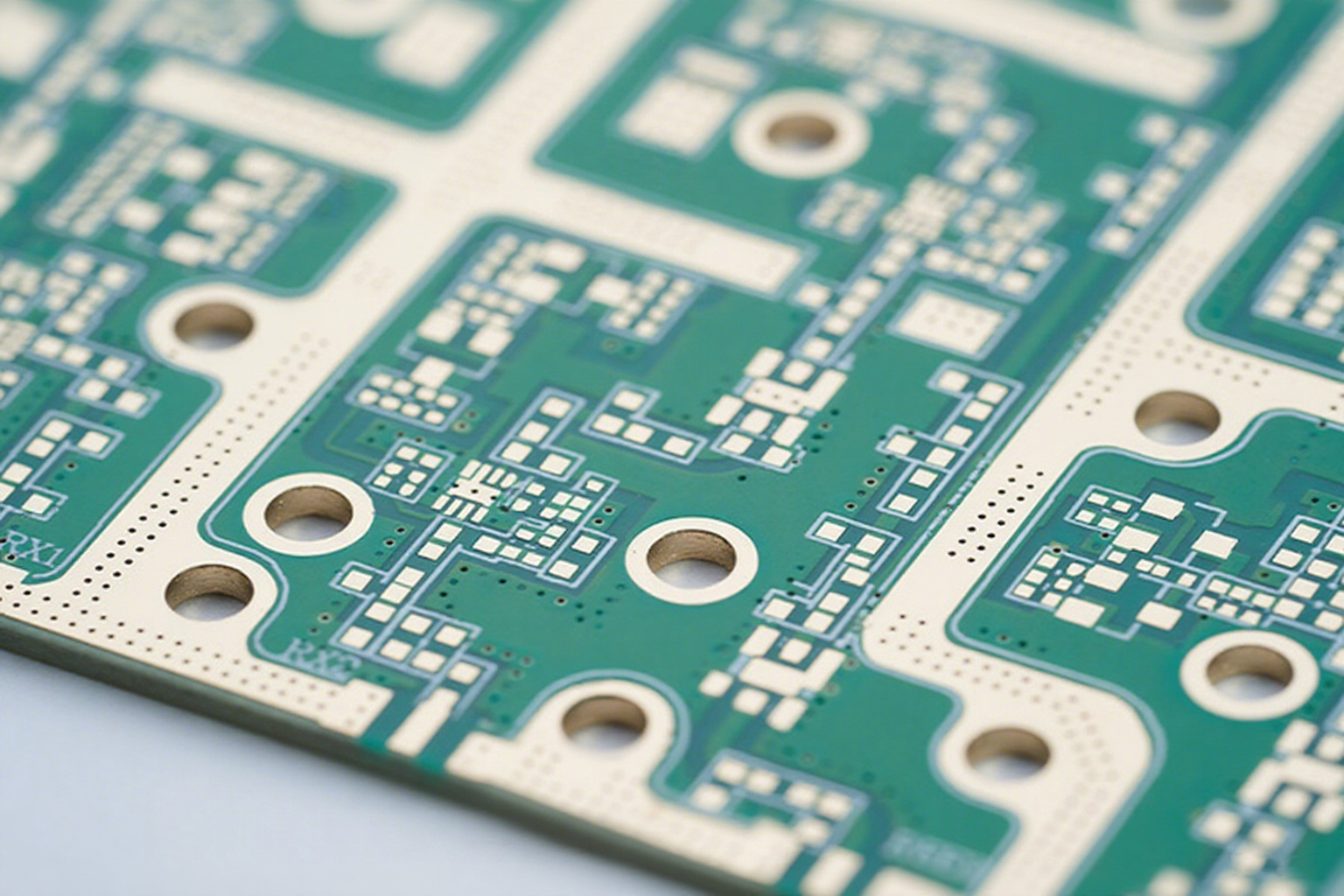
Layout decides how much of the simulated performance survives into hardware. The RF route needs a controlled impedance, and the fabricator has to be given the stackup and the target so the trace width can be calculated for the material actually used. The reference plane under the route has to be continuous; a split under a matched line creates a discontinuity that no component value can repair.
Vias are inevitable at some point, and each one is a small impedance step. They should be used sparingly, and where a transition is needed, ground vias placed close to the signal via give the return current a short path and reduce the disturbance. Keeping the matching components right beside the port they serve matters as much, because a long trace between the network and the device adds reactance that shifts the match. The choice between microstrip and stripline affects how sensitive the route is to the environment around it.
Tuning On The Bench
Measurement closes the gap between the simulation and the hardware. A vector network analyser sweep of S11 and S21 gives the actual complex impedance at the port, and that data is what the tuning is based on. If return loss is out of specification, the first question is where the problem lies: a trace whose impedance drifted during fabrication, a connector that adds its own reflection, or a network whose values are simply wrong.
A time domain reflectometer answer that question quickly, because it shows impedance against distance along the path and makes the offending section obvious. Without it, the temptation is to change components one by one, which is slow and often ends with a network that has been tuned around a solder defect. Soldering faults, stray solder on a pad and a connector that is not fully seated all produce a signature that looks like a mismatch, and they should be excluded before any component value is changed.
Choosing A Network Topology
Which matching network to use depends on the bandwidth and the impedance transformation required. An L network uses two elements and is compact, which suits a narrow band where the transformation ratio is modest. Pi and T networks add a third element and allow the loaded quality factor to be set, trading bandwidth against selectivity. A quarter wave transformer suits a fixed frequency and a defined transformation ratio, but it occupies more board area.
For a narrow band design the element values can be estimated on a Smith chart and then refined by measurement. A wideband design cannot be optimised at the centre frequency alone; the return loss has to be checked across the whole band, and it is common to trade some match at the centre for a flatter response at the edges. Passing the signal through the network also costs insertion loss, which is why routing a high frequency path without unnecessary length is worth the effort.
Closing The Loop
Tuning is an iterative process rather than a single adjustment. The starting state is measured, the network is changed, the S parameters are re-measured, and the system level figures such as gain, noise and output power are checked at the same time. Improving S11 alone does not prove that the link is better, because a network that absorbs energy to flatten the match will cost output power.
The order of work matters: fix the process defects first, then the layout discontinuities, then the component values. Following that order keeps the design honest, and it leaves a record of what was changed and why, which is useful when the same board is built again. gopcb builds controlled impedance RF boards with documented stackups and impedance verification so that the hardware starts from the value the simulation assumed.
What The Fabricator Needs From You
A matched RF board is only as good as the information that accompanied it. The stackup, the layer that each controlled line sits on, the target impedance, the reference plane and the tolerance all belong on the fabrication drawing, together with a note that a coupon will be measured. Supplying the geometry alone and expecting the board house to infer the target is the most common reason a first article misses.
It is equally useful to say where the impedance does not matter. Marking the lines that must be controlled keeps the fabricator from spending effort, and panel area, on nets that are not part of the RF path. Where a controlled line has to change layers, the via design rules that apply to a high frequency stackup should be agreed in advance rather than discovered at first article.
FAQ
Is VSWR or return loss the better specification? Either can be used, since they describe the same condition. Return loss is easier to state across a wide range, and VSWR is more common in cable and antenna documents.
Why does my simulated match not appear on the board? Component parasitics, laminate tolerance and line width variation are the usual reasons. Including them in the simulation and checking the corners removes most of the surprise.
When is a matching network unnecessary? When the source, the line and the load already present the same impedance across the band of interest. In that case the network only adds loss.