Multilayer PCB Prototype Fabrication: 2 to 48 Layers
A multilayer PCB prototype order is a specification before it is a product. Layer count, panel size, drill diameter, copper weight, impedance tolerance and surface finish all have to be stated before the first panel is built, and each of them changes the price and the lead time in a predictable way.
This article walks through the parameters that a prototype quotation is built from, the practical limits that decide what is achievable, and the choices that keep a prototype process stable when the design moves into volume production later.
What the Layer Range Really Means
A multilayer PCB can be built anywhere from two to forty-eight layers, but the useful range for most products is much narrower. Four and six layers cover the majority of control, power and instrumentation boards. Eight to twelve layers appear when a design needs several dedicated routing layers plus solid reference planes. Beyond sixteen layers the constraint stops being the artwork and becomes the lamination cycle.
Each additional layer adds a pressing operation, and each pressing operation adds a chance for misregistration, resin starvation or a wrinkle in the prepreg. Prototype fabrication is therefore priced by the number of press cycles, which is why high layer counts are quoted with longer lead times even when the artwork is straightforward. Most teams find that a multilayer prototype requirement is settled by the reference planes rather than the routing density. The sensible question is not how many layers are possible but how few layers will carry the design with an uninterrupted reference under every high-speed net.
Panel Size, Thickness and Material Choice
Prototype panels are usually built on a standard working panel and then routed out, so a board that fits a common panel format costs less than one that does not. Very large outlines, above roughly half a metre in either direction, begin to consume panel area inefficiently and can force a dedicated tooling setup. Very small boards have the opposite problem, since handling and registration dominate the cost.
Finished thickness is normally specified between 0.2 and 3.8 millimetres for a prototype run, and the value interacts with the layer count. A twelve-layer board at 1.0 millimetres has thin dielectric layers that demand tighter control in lamination. The laminate choice follows the same logic: standard FR-4 covers most work, while ceramic-filled, high-frequency or metal-core materials are specified only when the electrical or thermal requirement justifies the extra processing.
Minimum Features: Hole, Trace and Spacing
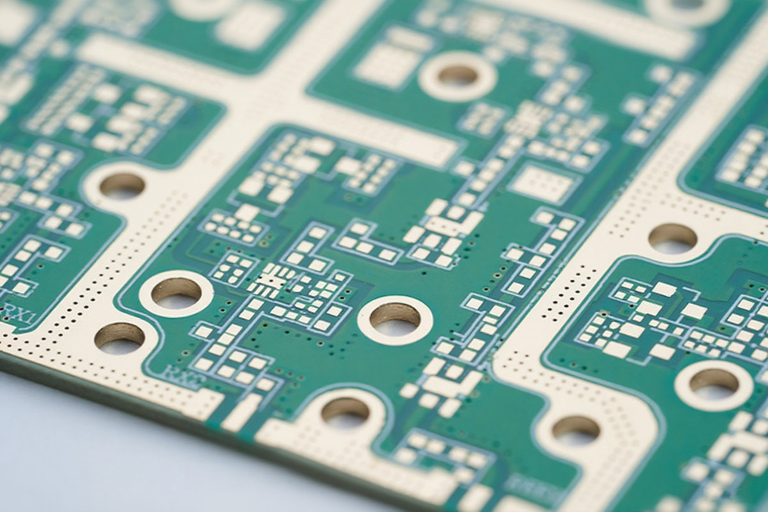
The minimum finished hole size is a good measure of how aggressive a design is. A 0.2 millimetre hole is achievable in production, but holes at that diameter are usually reserved for via-in-pad or high-density escape work, because the plating aspect ratio becomes the limiting factor. A thicker board with the same hole size is harder to plate reliably than a thin one.
Trace width and spacing are quoted together, typically at four mils for prototypes, and the dielectric spacing has to support the voltage as well as the process. Impedance control is the parameter that ties the two together: a quoted tolerance of plus or minus eight to ten percent is realistic, and it is achieved by controlling dielectric thickness and trace geometry, not by measuring the finished board and hoping.
Impedance Control Tolerance and What Drives It
Impedance control starts in the stack-up and ends in the coupon. The fabricator must know the target impedance, the layer on which each controlled net runs, and the reference plane for that layer. Without those, the CAM engineer is guessing, and the measured result on the finished board will scatter accordingly.
Once the stack is defined, the tolerance comes from the variation in dielectric thickness and in etched trace width. Both are process parameters the fabricator controls through lamination pressure, prepreg selection and etch compensation. That is why a request for tighter impedance control is really a request for tighter process control, and it is priced that way.
Surface Finish Options and How to Choose
The surface finish protects the copper between fabrication and assembly and decides how well the solder wets during reflow. Hot air solder levelling is inexpensive and gives a long shelf life, but the surface is not perfectly flat and it is unsuitable for fine pitch. Immersion gold, applied over nickel, is flat and reliable at fine pitch, and it is the usual choice for boards that will be stored before assembly.
Organic solderability preservatives are the cheapest flat option, with the shortest shelf life and the greatest sensitivity to handling. Immersion silver and hard gold cover the cases in between. The choice between lead-free and leaded processes is a separate decision that should be made at the same time, since it affects the finish, the solder alloy and the reflow profile together.
Electrical Test: Flying Probe and Fixture Testing
Bare board testing exists to catch opens and shorts before components are placed, when the board is still cheap to replace. Flying probe testing needs no tooling and is the natural choice for prototypes, because the probe program can be generated from the netlist and changed as the design changes.
Fixture testing becomes economical once the quantity is high enough to amortise the fixture, and it is much faster per board. Either way, the test program is only as good as the netlist it was built from, so a design that leaves unused pads unconnected deliberately should mark them as no-connect in the schematic rather than leaving the tool to interpret them. Mild electrical test alone is not enough for fine geometry; the design rules that keep a board manufacturable are what stop the defects being created in the first place.
From Prototype to Volume: Keeping the Process Stable
The prototype is a process experiment as much as a product sample. The parameters that were used to build it, from the stack-up to the etch compensation and the lamination cycle, should be recorded, because they are the starting point for the production version. A fabricator who can quote the same stack for volume has already solved most of the transfer problem.
Two things commonly change between prototype and volume and cause trouble. The first is panel utilisation, which can drive a different panel layout and therefore a different copper distribution. The second is the surface finish, which is often switched to save cost. Both should be treated as engineering changes and verified on a first article rather than assumed to be equivalent.
Feeding the Result Into Assembly
Once the bare boards have passed test, the same panel usually moves into surface mount assembly, and the fabrication decisions continue to matter. Solder mask thickness over the pads, the flatness of the finish and the accuracy of the outline all affect placement and reflow. A panel that was in tolerance for fabrication can still give poor assembly yield if the mask dam is too narrow between fine pitch pads.
The order of the assembly line is worth understanding even for a pure fabrication order, because it explains the tolerances that matter. Paste printing, placement, reflow, cleaning, inspection and rework each add their own variation, and inspection cannot improve what the printer and the oven already produced. Keeping the fabrication and assembly data consistent, including the same pad definitions in both, removes an entire class of avoidable defects.
FAQ
How many layers should a prototype actually use? The fewest that allow every high-speed net to reference a continuous plane and every power net to reach its load with an acceptable drop. Adding layers to make routing easier usually costs more than solving the stack-up properly.
Is a tighter impedance tolerance always worth paying for? Only when the channel budget is genuinely tight. A tolerance of plus or minus ten percent is adequate for most digital interfaces, while a narrow analogue or radio front end may need the tighter grade. State the requirement per net class rather than for the whole board.
What should be specified on the fabrication drawing? Layer count, finished thickness and tolerance, laminate type, copper weights, minimum trace and space, impedance targets by layer, surface finish, solder mask and legend colour, outline tolerance and the test requirement. Anything left unstated will be decided by the fabricator.