PCB Dimensions: Thickness, Tolerances and Edge Clearance
PCB dimensions are the set of mechanical parameters that decide whether a board can be built, assembled and fitted into its enclosure: length and width, thickness, copper weight, hole size, outline tolerance and the clearance between the outermost copper and the board edge. They receive far less attention than the schematic, and they are responsible for a large share of the problems that appear after the design is released.
Outline Sizes and What Drives Them
There is no single standard board size, because the size follows the product. Wearable and module designs sit in the tens of millimetres, industrial controllers typically occupy 100 to 200 mm on a side, and backplanes for switching and computing equipment run to several hundred millimetres and beyond. What is standard is the fabrication equipment, which sets an upper limit on the panel rather than on the board.
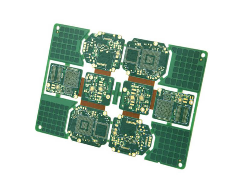
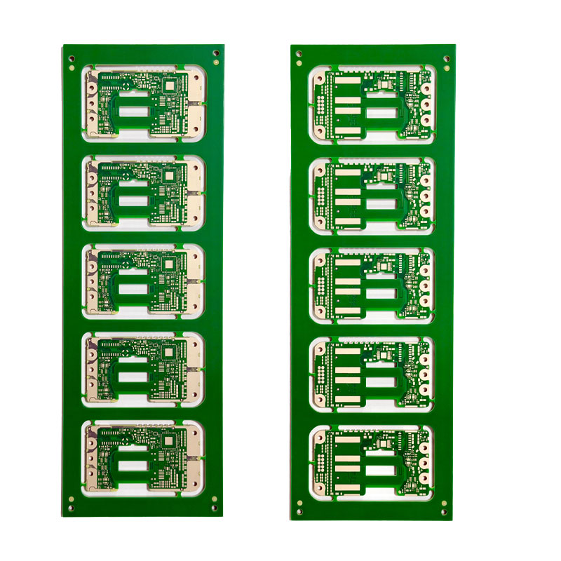
The practical constraint is panel utilisation. Boards are produced in a panel that is a fixed size for the fabricator, and the way the boards are arranged on it determines how much material is wasted. A board dimension that divides the available panel area poorly costs money on every unit for the life of the product, which is why adjusting an outline by a few millimetres during prototyping can be worth more than a supplier negotiation later.
Board Thickness
Thickness is dominated by one value: 1.6 mm, which is the de facto standard for rigid boards. It is stiff enough for most assemblies, compatible with standard connectors and card guides, and it is the thickness at which material is cheapest and process windows are widest. Most consumer and industrial products use it without further thought.
Other thicknesses are used for a reason. Thin boards of 0.4 to 1.0 mm suit compact products and are common in modules and cards where height is constrained, but they flex more during assembly and may need a carrier. Thick boards of 2.4 mm and above resist bending and are used for heavy backplanes, high current assemblies and boards that must tolerate a large connector insertion force.
Thickness tolerance is normally quoted as a percentage, with ten percent being typical, which on a 1.6 mm board allows roughly 1.44 to 1.76 mm. Where that spread matters, for a card guide or a press fit connector, a tighter tolerance can be specified, at the cost of lower lamination yield. The relationship between thickness and stackup is described in layer stackup planning.
Tolerances That Matter
Outline tolerance is usually quoted as plus or minus 0.1 mm for a standard routed board and plus or minus 0.05 mm for a precision process. The number is dominated by the routing method and by the dimensional movement of the laminate, not by the accuracy of the cutter, so a board with a tight outline requirement and a large area is difficult to hold.
Hole tolerance is the second dimension that matters, and it differs by process. A mechanically drilled hole holds about plus or minus 0.075 mm, while a laser drilled microvia holds around plus or minus 0.025 mm. Copper thickness is usually quoted to within ten percent. For connectors, press fit pins and anything else that has to fit a mating part, the tolerance that matters is the finished hole size after plating rather than the drill size quoted on the drawing.
Holes and Vias
Through holes range from about 0.2 mm up to 1 mm and beyond for connector pins and mounting hardware. The rule that governs their design is not the drill diameter but the ratio of board thickness to hole diameter: a deep hole in a thick board is hard to plate uniformly, so a small via in a thick board is a reliability risk rather than a density improvement.
Microvias of 0.075 to 0.15 mm are used in high density designs, usually in the outer layers of an HDI stack, and they allow via in pad placement that frees routing area under fine pitch packages. Their design follows the same registration and annular ring rules as any other via, and the choices are covered in via design rules.
Edge Clearance
Edge clearance is the distance from the outermost copper to the board outline, and it protects the board during routing and depaneling. A minimum of 0.25 mm is common and 0.5 mm is a comfortable recommendation, because the cutter leaves a small radius and the laminate can chip at an unsupported edge. Copper that runs too close to the edge can be exposed by the cut or damaged by handling after it.
High voltage designs increase that distance deliberately, because the clearance to the edge is part of the creepage path, and mounting hardware or a chassis can bring a conductive surface close to the board edge. Outline and edge features generally should be planned with the enclosure in mind, as described in board outline and mounting design.

What Drives Cost
Size, thickness and tolerance each move the price, and they compound. A larger board consumes more material and more processing time; a thicker board needs more prepreg and a longer lamination cycle; a tighter tolerance adds inspection and reduces yield. High density features such as microvias and multiple lamination cycles sit on top of all three.
The design advice that follows is simple. Use a standard thickness unless there is a reason not to, avoid specifying a tight tolerance on a dimension that does not need one, and arrange the outline so that the panel is well utilised. Reviewing those three decisions with the fabricator before the design is frozen is cheaper than correcting them afterwards.
IPC References for Dimensions
The industry relies on a family of documents rather than a single dimensional standard. IPC-2221 covers general design, IPC-6012 covers the performance requirements of rigid boards including hole and outline tolerance, IPC-A-600 defines what is acceptable visually, and IPC-6013 does the same job for flexible boards. Where a drawing is silent on a dimension, one of those documents normally supplies the default.
Citing them has a practical benefit beyond compliance. A drawing that references IPC-6012 for hole tolerance and IPC-A-600 for appearance removes the argument about whether a given amount of edge roughness or a slightly oversized hole is a defect, because both sides are working from the same acceptance criteria. For products sold internationally it also satisfies the documentation expectations of most original equipment manufacturers, who will ask which standards the board was built to before they ask about price.
FAQ
What is the most common PCB thickness? 1.6 mm, or 62 mil, is the de facto industry standard. It is mechanically adequate for most assemblies, compatible with standard hardware and the cheapest thickness to produce.
How large can a PCB be manufactured? Most fabricators can handle panels in the region of 500 mm square, while large facilities support boards of 1200 mm by 650 mm and occasionally more. The limit is the press and the drilling equipment rather than the material.
What tolerance should be specified on the board outline? Plus or minus 0.1 mm is standard for a routed board and is adequate for most products. Specify 0.05 mm only where a mating part genuinely needs it, because the tighter figure costs yield.
How close can copper be to the board edge? A minimum of 0.25 mm is workable and 0.5 mm is recommended for a routed board. High voltage designs often need several millimetres because the distance to the edge forms part of the creepage path.