PCB Manufacturing Process: From Gerber to Finished Board
A circuit board passes through dozens of controlled steps between the design file and the finished panel, and most of them cannot be verified by inspecting the final product. Understanding the sequence helps a designer see which of their decisions are easy to accommodate and which ones create risk, and it explains why a small change in a drawing can produce a large change in the price.
Data Preparation
The process begins with the design data: Gerber files for each conductive and non conductive layer, a drill file, and a specification for the stackup, the material and the finish. The fabricator converts this into production data, adds the panel frame, adds coupons and tooling features, and compensates the artwork for the way each process will modify it.
Compensation is where experience shows. Etching removes metal sideways as well as downwards, so the artwork is drawn slightly wider than the finished trace, and plating adds thickness that changes the final dimension. The designer never sees these adjustments, but a design that leaves too little margin for them becomes unmanufacturable.
Inner Layer Imaging and Etching
The inner layers of a multilayer board are produced first. A copper clad laminate is cleaned, laminated with photoresist, exposed through the artwork and developed, leaving resist only where copper should remain. The panel is then etched, the resist is stripped, and the layer is inspected and measured.
Plating is followed by the outer layer imaging and etching, described in the material on PCB design and fabrication. Each inner layer is then bonded to the others in the lamination press, with prepreg between them. The pressing cycle controls temperature, pressure and time, and it determines the final thickness and the amount of resin flow. After lamination the panel is a single solid board, and the inner layers can no longer be adjusted.
Drilling
Holes are drilled by a numerically controlled machine using a programme derived from the drill file, with a different tool for each diameter. The drill bit count is limited by the tool changer, so a design with many distinct hole sizes costs more and takes longer.
Hole quality is critical, because a rough or smeared wall prevents the plated copper from adhering to the inner layer. For epoxy laminates the smear is removed chemically, and for polyimide the process is more aggressive. The aspect ratio of the hole determines how difficult it is to plate reliably, which is why a design rule limits how deep a small hole may be.
Plating
Plating deposits copper inside the holes to connect the layers and, in some processes, adds thickness to the surface conductors. The step begins with a thin conductive layer deposited chemically over the entire panel, followed by electroplating in a bath whose chemistry is carefully balanced.
The organic additives that control the deposit are the difference between a uniform barrel and one that is thin in the middle, and the plating topic is treated in detail under electroplating additives for PCB. Plating is followed by the outer layer imaging and etching, or by a pattern plating sequence in which the plating happens after imaging.
Solder Mask, Legend and Finish
Solder mask is applied as a photoimageable coating, exposed through artwork that defines the openings and developed. The registration of the mask to the copper is what determines the minimum dam width, as described in the discussion of PCB design guidelines for manufacturability.
The legend is printed next, usually through a screen, and cured. The surface finish is then applied to the exposed pads: hot air levelling, immersion tin or silver, or electroless nickel immersion gold. Each has a different process and a different effect on the pad geometry and shelf life.
Outline, Inspection and Test
The board outline is routed or punched, and any special machining such as a cavity or a plated edge is performed. Electrical test follows, using a flying probe or a dedicated fixture, to verify continuity and isolation on every net.
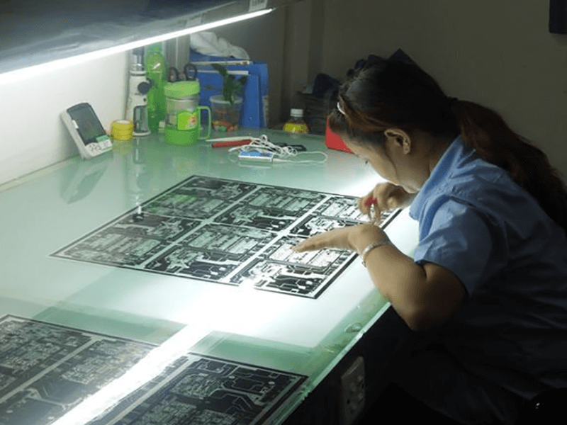
Inspection covers the visual and dimensional aspects: automated optical inspection of the surface, microsection of coupons to confirm plating thickness and layer registration, and a final visual check under magnification. The coupons are important because they carry the evidence that the process was in control, which is the only record that survives for a board that is inspected destructively.
Panelisation and Its Effect on Cost
Boards are produced in panels because the process equipment works on a standard size. The number of boards that fit on a panel, and the amount of material left over, has a direct effect on unit cost, so the outline and the panel arrangement are economic decisions as much as manufacturing ones.
Break away tabs, tooling holes and fiducials are added to the panel frame, and their placement has to suit both the fabrication equipment and the assembly line. A panel that suits one may need to be re-drawn for the other, which is why the two suppliers should be involved before the design is finalised.
Where Design and Process Meet
The steps that punish a design are the ones that cannot be corrected later. Lamination fixes the stackup, drilling determines the aspect ratio, and plating determines the barrel quality. A design that respects the process limits at those three points avoids most of the expensive outcomes.
The rest is margin. Minimum line width, minimum annular ring, minimum drill size and minimum spacing should all be generous enough that ordinary process variation does not consume the whole allowance. Designs that use the absolute minimum everywhere achieve the smallest board at the highest cost per unit, which is rarely the right trade. A design that uses ordinary rules and accepts a slightly larger board usually costs less in total than one that squeezes every dimension to its limit and loses yield doing it. That is as true of the panel frame as it is of the copper, and the two decisions are made at the same time.
Auditing a Supplier
Useful questions concern the process rather than the equipment list: what plating thickness is held and how it is verified, how the etch compensation is derived, what the registration tolerance is on a build like this one, and how coupons are retained.
The answers reveal whether the shop operates by control or by inspection. A shop that measures and records is in a position to detect drift before it produces scrap, and it can show a customer the evidence. That is the difference between a quotation that is cheap today and one that is cheap over the life of the product, and it is the question worth asking before price is discussed at all.
FAQ
How long does PCB manufacturing take? A standard multilayer board is typically seven to fifteen working days, with the time dominated by lamination, plating and test rather than by any single step.
Can a design be changed after the order is placed? Only before the artworks are produced and the inner layers are etched. After lamination the change is a new board.
Why does the fabricator change my artwork? To compensate for the way each process modifies the pattern. The compensation is applied so that the finished board matches the design intent rather than the drawing.