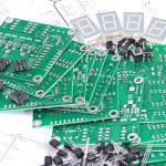
PCB Prototype Order: Every Field You Must Specify
A PCB prototype order is a specification, and the fabricator will build exactly what the specification says rather than what the designer intended. Every field that is left blank is filled in with a default, and the default is chosen for cost rather than for fit. Writing the fields out explicitly is therefore less about paperwork than about controlling the handful of choices that decide whether the boards can be assembled.
What the Fabricator Needs From You
The requirements come in two halves. The design side is the responsibility of the engineering team: selecting part numbers deliberately so that cost is controlled, checking unusual footprints before they reach the fabricator, running simulation and electrical checks, and completing the signal integrity work so the board behaves as designed. The manufacturing side belongs to the fabricator: reading the supplied data and flagging anything unbuildable, running the process in a controlled way at every step, improving yield, and raising an engineering question rather than making an assumption when something in the data is ambiguous.
That last point is the one that decides the schedule. A fabricator that stops to ask adds a day; a fabricator that guesses adds a re-order. Supplying the specification up front moves the questions to the start, where they are cheap.
Substrate and Thickness
The substrate is the first field. The common choices are FR-4 glass cloth, the composite laminates such as CEM-1 and CEM-3 with a partial glass content, paper-based grades such as 94VO and 94HB, and the special substrates: aluminium, copper, high-frequency laminate, and polyimide film for flexible circuits. The choice follows from the thermal and electrical requirement rather than from price alone, because a cheaper laminate that changes dimension under load is not cheaper overall.
Thickness is the second field and is usually quoted as the finished board thickness. The standard range runs from 0.15 mm through 0.2, 0.4, 0.6, 0.8, 1.0, 1.2, 1.6, 2.0, 2.2, 2.4, 3.0, and 3.2 mm and above. Connector heights, card guides, and enclosure features are all designed around this number, so it should be stated rather than left to the shop to infer from the stackup. The way the laminate and stack are specified together is covered in PCB design and fabrication.
<img src="https://www.gopcba.com/wp-content/uploads/2024/09/Through-Hole-PCB-Assembly1.png" alt="PCB prototype order specification sheet with substrate and copper weight” />
Copper Weight, Mask and Legend Color
Copper weight determines both the current capacity and the minimum feature size, since thicker foil etches with more undercut and forces wider traces and gaps. The common weights are 0.5, 1, 1.5, 2, 3, 4, 5, and 6 ounces. A design that needs the current capacity of two ounces should state it, because a fabricator who substitutes one ounce to save cost changes the resistance and the thermal behavior at the same time.
Solder mask color and legend color are functional choices dressed as cosmetic ones. Green remains the default because it gives good contrast for inspection and is the best-understood process, and dark colors reduce the contrast that automatic optical inspection relies on. White, black, purple, yellow, matte black, and blue are all available. Legend is normally white, black, or yellow. The color affects how well the board can be inspected and how easy rework is, which is why it belongs in the specification rather than in an email after the fact.
Via Treatment and Surface Finish
Via treatment has four common options: opened, tented, plugged with ink, and filled. The difference matters most when a via sits under a component land, where the requirement is a flat and closed surface, and least when no device sits over the hole. Specifying it prevents the shop from applying the cheapest treatment to a via that needed a better one.
Surface finish is the field with the widest range of consequences. Bare copper, organic solderability preservative, immersion gold, immersion tin, immersion silver, lead-free hot air leveling, electroplated gold, and hard gold are all in routine use, and each pairs with a different assembly process and a different shelf life. Because the finish also interacts with the solder alloy, it should be chosen together with the assembly plan, and the comparison in lead-free versus leaded solder is part of the same decision.
Quantity, Panelization and Lead Time
Quantity is quoted as a number of finished pieces, but the shop thinks in panels, so the number has to divide into whatever arrangement it chooses. A quantity that leaves a partial panel costs more per piece than one that fills the panel, and the panel size is chosen by the shop unless the design constrains it.
Delivery is specified as standard or expedited, and it is worth deciding deliberately rather than by default, because expediting a standard process costs far less than expediting a non-standard one. Where a design needs a special substrate or an unusual finish, the lead time is driven by material availability rather than by the line. The sequence a prototype follows from layout to volume production is described in PCBA development process.
Impedance and Special Processes
If the design needs impedance control on specific nets, the requirement has to be stated with the target value, the tolerance, and the layers it applies to. A single number for the whole board is not a specification, because the geometry differs between outer and inner layers and the fabricator needs to know which net is which.
Special processes are the fields most often forgotten. Vias in pad, blind and buried vias, and countersunk holes each change the process flow and each has to be declared. Countersinking removes material from the pad and needs a depth tolerance, while blind and buried vias require sequential lamination, which is a different build entirely. Any requirement that the standard flow cannot produce belongs on the specification, even when it seems obvious from the artwork.
Test Method
The last field is how the boards will be verified. Visual inspection suits simple, low-density boards, while flying probe test checks continuity and isolation on every net and is the normal choice for anything dense. The choice carries a cost and a schedule implication, and it should be made with the assembly plan in mind, because a board that will be assembled automatically needs its nets verified before assembly rather than after it.
Putting all of this on one page is the whole point. A specification sheet of a dozen lines replaces a week of correspondence, and it makes the order reproducible: the second batch is built from the same fields as the first, so any change in behavior between batches points at the process rather than at an unstated assumption.
FAQ
What is the most commonly forgotten field? The via treatment. Tented, plugged, and filled vias look identical in the artwork but require very different process steps.
Does mask color really matter? Yes, for inspection. Green offers the best contrast for automated optical inspection, and dark colors reduce it, which changes how much manual review the board needs.
How should a quantity be chosen? In multiples that fill the panel the shop will use. A quantity that leaves a partial panel costs more per piece than one that fills it.
Why state impedance if the stackup is already defined? Because the fabricator needs the target value, the tolerance, and the specific layers. A stackup alone does not say which nets are controlled.