In-Circuit Test on PCBs: Fixtures, Test Points and Coverage
In-circuit test checks the components on an assembled board one at a time: it measures a resistor, verifies the polarity of a diode, confirms that a capacitor is present and that its value is within tolerance, and detects a short or an open between adjacent nets. It does so with the board powered down in most cases, which is what makes it fast and repeatable.
Its value is coverage of the defects that functional test cannot localise. A board that fails a functional test tells the engineer that something is wrong; an in-circuit test tells them which component, which pin and which net.
What In-Circuit Test Does
The test applies a signal or a bias to a net through a probe and measures the response. Because the board is not powered, the surrounding components are effectively isolated by the diode junctions inside the semiconductors, which allows an individual part to be characterised inside a populated circuit.
Guard techniques extend that isolation where the parallel paths cannot be ignored. By driving a second net to the same potential, the current through an unwanted path is cancelled, and the measurement describes the component of interest rather than the network around it.
<img src="https://www.gopcba.com/wp-content/uploads/2026/08/1768208893-quick-turn-pcb-assembly.webp" alt="Bed of nails test fixture pressing onto a populated PCB” />
Bed of Nails Fixtures
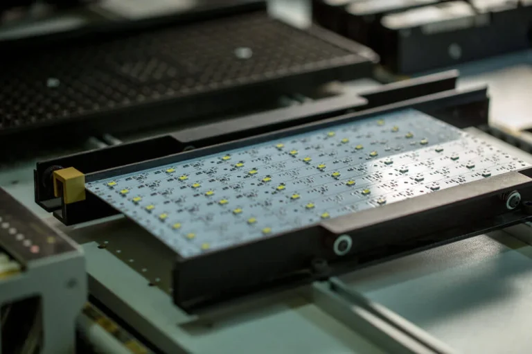
The traditional implementation is a fixture with a field of spring loaded probes, one for each test point, pressed against the board at once. All of the nets are accessed simultaneously, so the test runs in a second or two and every board in a production run receives the same measurement.
The fixture is specific to the board. It has to be designed, machined and wired, and its cost is justified by the production volume. A change to the layout that moves a test point requires a new fixture or at least a modification, which is why the test point positions are frozen early in a high volume programme.
Flying Probe Testing
A flying probe machine moves a small number of probes to each test point in turn, so it needs no fixture and no dedicated hardware. That makes it ideal for prototypes, for low volume production and for boards whose layout is still changing.
The trade is time. Because the probes travel between measurements, a flying probe test takes minutes rather than seconds, and the cost per board is correspondingly higher at volume. Access from both sides is required for a double sided assembly, and the machine needs a stable, flat board to probe reliably.
Test Point Design
A test point needs a defined area of exposed copper, clear of the solder mask and clear of any component that the probe or the fixture might touch. Its size follows the probe diameter, the placement accuracy of the machine and the registration tolerance of the mask.
The test point should also be placed where the probe can reach it. A point under a tall component, under a shield can or too close to a connector cannot be probed, and the resulting loss of coverage is discovered at test development rather than at the design review unless the layout is checked for access.
Coverage and Access
Coverage is the fraction of the possible defects that the test can detect, and it is calculated from the net access and the component list. A net with no test point is a net whose opens cannot be found, and a component with both terminals on inaccessible nets cannot be measured at all.
In practice coverage of 85 to 95 percent is achievable on a well designed board, and the shortfall is usually in the high pin count devices where the nets are buried in a ball grid array. Those devices are covered by boundary scan or by functional test rather than by probing.
Test Development and Programming
The test program is generated from the netlist, the bill of materials and the CAD data, and it is then debugged on a golden board. The debug corrects the guard values, the tolerances and the measurement order, and it is the step in which most of the initial cost sits.
Fixture design, program generation and debug are the three investments, and all three are reduced by good design data. A library of validated component models and a complete netlist shorten the process considerably compared with a program built from a partial data set.
Comparison with Functional Test
In-circuit test verifies the assembly; functional test verifies the product. The first finds a wrong resistor, the second finds a firmware problem or a thermal issue. Most production lines use both, with in-circuit test earlier in the flow so that a board with a misplaced component does not consume functional test time.
Where the product is simple, functional test can cover the assembly defects and the in-circuit step is omitted. Where the product is complex and expensive, the in-circuit test pays for itself by removing a board from the line before the costly test stage.
Design Rules and Documentation
Provide test points on every net that matters, keep them away from tall components and from the board edge, place them on a regular grid where the fixture design allows, and give them a uniform size so that the same probe can be used everywhere. Mark the test point layer in the fabrication data so that the mask opening is applied.
gopcb produces boards with test point pads, mask openings and the surface finish that probing requires, and can supply the net and coordinate data that a fixture shop or a flying probe programme needs.
Diagnostics After a Failure
An in-circuit test that fails produces a diagnostic message that names the net and the measurement, and the quality of that message decides how quickly the board is repaired. A test that reports only a failure forces the technician to investigate the whole circuit, while a test that reports a specific component with an expected and measured value allows the repair to be made immediately.
Good diagnostics come from the program rather than from the machine. Guard values that isolate the component, tolerances that reflect the real measurement uncertainty and a clear naming convention for the nets all reduce the diagnostic time, and the investment is repaid at the first production run because the repair station is where the labour cost accumulates.
When Not to Use In-Circuit Test
There are products for which the test is not economical. A very small board with a handful of components is covered by functional test at lower cost, and a board that is entirely covered by conformal coating or by an encapsulant cannot be probed at all after that step. In those cases the test has to happen earlier in the flow or be replaced by another method.
A board that is produced in very low volume is another case, because the fixture cost cannot be amortised. A flying probe avoids the fixture and is usually the right answer for a prototype or a short run, even though the test time per board is longer, because the total cost over the small quantity is lower than a dedicated fixture that is used twice.
FAQ
Do I need test points if I use a flying probe? The probe still needs copper to touch, so test points remain necessary. What the flying probe removes is the need to design a dedicated fixture.
Can in-circuit test measure a component in a populated circuit? It can, using guard techniques and the fact that the board is unpowered, but the accuracy depends on the surrounding network and on the tolerance the test is asked to hold.
Is in-circuit test a replacement for functional test? No. They detect different classes of defect, and a product with any complexity needs both, with in-circuit test placed earlier in the flow.
Related reading: PCBA development process, silkscreen and legend design, PCB design quality characteristics, and PCB manufacturing tolerances.