IC Substrate and PCB: Structure, Materials and Process
An IC substrate and a printed circuit board are made with similar equipment and similar chemistry, and they are often confused in conversation. They are different products with different requirements: a PCB carries components and connects them across a system, while an IC substrate carries a die and connects it to the package and to the board beneath.
The distinction matters because the substrate is built to a much finer geometry and to a much tighter tolerance, and those requirements change the material, the process and the cost.
What Each One Is
A printed circuit board is a laminate structure with drilled and plated through holes, etched copper patterns and a surface finish, populated with packaged components. Its features are measured in tens of micrometres at the finest, and its layer count is typically between two and thirty.
An IC substrate is a much denser structure that carries a bare die. Its features are measured in single digit micrometres, its layers are thin and numerous, and it is designed to match the die’s pad pitch rather than a component footprint.

Feature Size and Routing Density
The line width and spacing on a PCB are limited by etching and by the laminate, while a substrate uses semi additive processes that build the conductor rather than etching it away. That difference is what allows a substrate to reach a line width that a conventional board cannot hold.
The density requirement comes from the die. A high pin count die presents pads at a pitch of a hundred micrometres or less, and escape routing from that field requires several layers of very fine conductors before the pitch can be relaxed to the board level.
Materials and Their Properties
A substrate material is chosen for a low dielectric constant, a low loss and a coefficient of thermal expansion close to silicon. The expansion match reduces the stress on the solder bumps and the microbumps that connect the die, which is a reliability requirement rather than a performance one.
A board material is chosen for a wider set of requirements: mechanical strength, cost, process compatibility, flame retardance and, at high frequency, loss. The expansion match to a die is not part of the specification because the die is not attached to it directly.
Manufacturing Processes
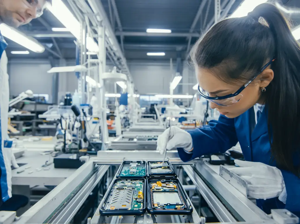
The substrate process uses panel or strip formats, build up layers with microvias, fine line imaging and a surface finish suitable for wire bonding or flip chip attachment. The process control is tighter, the inspection is more detailed and the yield is lower, which is reflected in the cost per unit area.
The board process is more forgiving, larger, faster and cheaper per square metre, and it is optimised for volume rather than for the finest geometry. The two processes share a language but not a capability, and a feature that is routine on a substrate can be impossible on a board.
Electrical Performance
The electrical requirements of a substrate are dominated by the interface to the die: a large number of short, high bandwidth channels with a controlled impedance and a very low loss. The board carries the same signals over a longer distance, at a lower density and with more tolerance for loss.
Where the two meet, at the package to board interface, the design has to manage the transition. A ball grid array on the substrate side and a board level footprint on the other are different structures, and the transition between them is where the impedance discontinuity and the mechanical stress concentrate.
Cost Structure
A substrate costs many times more per unit area than a board, and the difference grows as the density rises. The cost is driven by the fine line process, the thin materials, the low yield and the inspection intensity.
The board cost is driven by area, layer count and the number of process steps, with a much lower cost per unit area. A design that moves function from the substrate to the board reduces cost, provided the density and the electrical performance allow it.
Where Each One Is Used
A substrate appears wherever a die has to be connected to the outside world in a package: processors, memory, radio frequency modules, sensors and power devices. A board appears in every product that contains more than one package or that has to connect a package to connectors, power and passive components.
In most products both are present, and the engineering decision is where to draw the boundary between them. Drawing it higher, with more of the routing inside the package, costs more but saves board area and improves the electrical performance in the critical channel.
Design Rules and Documentation
The design rules are not transferable between the two. A substrate drawing specifies the die pad pitch, the bump layout, the build up sequence and the finish for wire bonding, while a board drawing specifies the stackup, the impedance targets, the hole sizes and the assembly footprint.
gopcb builds high density boards and works with package substrates and substrate-like processes, and can advise where the boundary between the two should sit for a given die, channel budget and product cost.
The Interface Between Substrate and Board
Where a packaged die meets the board, the two technologies have to cooperate. The package presents a ball grid array at a pitch that the board can escape, and the board provides the reference plane, the power distribution and the thermal path for the package above it. The design of that interface is often the difference between a product that works and one that works only in the laboratory.
The electrical challenge is the transition. A signal leaves the substrate through a ball, travels through a pad and a via on the board, and continues to its destination. Each of those steps changes the local geometry and produces a reflection, and the cumulative effect at a high data rate is significant. The board is usually designed with the package vendor model rather than with a generic footprint, and the via structure under the package is optimised for the transition rather than for density alone.
Cost per unit area is not the only comparison. The substrate carries the die and the short high bandwidth channels, where the loss per unit length is critical, while the board carries the longer channels where a lower cost material is adequate. Splitting the function correctly between the two is what keeps the product affordable without compromising the channel budget, and the split is usually decided early, before either layout begins.
FAQ
Is an IC substrate just a very fine PCB? It uses similar chemistry but a different process and different materials. The line width, the layer structure, the expansion match and the inspection requirements are all outside the range of conventional board fabrication.
Why does the substrate need to match the die expansion? Because the die is attached with bumps that are small and rigid. A large expansion mismatch between the die and the substrate stresses those joints during thermal cycling and cracks them.
Can a board be used instead of a substrate? Only where the die pad pitch and the channel requirements are within the board capability. For a high pin count die the escape routing and the expansion match are beyond what a conventional board can provide.
Related reading: high density interconnect PCB, any layer HDI PCB, optical module PCB design, and PCB manufacturing processes.