Reverse Engineering Legacy Hardware into Usable Design Data
Reverse engineering a circuit board means reconstructing usable design data from a physical sample. It is a legitimate engineering activity with a long history: legacy equipment that must be supported long after its documentation has been lost, a competitor product that must be understood rather than copied, or a board that needs modification when no source files exist. The technique is straightforward in principle and unforgiving in execution.
What Reverse Engineering Is Used For
The most common driver is documentation loss. Equipment built decades ago still runs production lines, and the original drawings may no longer exist in any accessible form. Rebuilding them from a physical board is often the only way to make a repair, a modification or a replacement possible.
Analysis is the second driver. Understanding how a design was implemented can inform a new product without infringing anything, provided the intent is study rather than copying a protected layout. Whatever the purpose, the output is a set of design files, and their accuracy determines whether the exercise produces value or a new set of problems.
Documenting Components Before Anything Is Removed
The first step is recording what is present. Every component, its value and its position should be written down, with particular attention to orientation of diodes and transistors and to the keying notch on integrated circuits. Photographs of each side of the assembly are worth taking in addition to the written record.
This stage cannot be repeated once the board is disassembled, so it deserves more care than the rest of the process combined. A single reversed diode in the record will produce a rebuilt design that is wrong, and the error will not be obvious until the resulting board is powered up for the first time.
Exposing and Imaging the Copper Layers
With the components removed and the pad holes cleared of solder, the board is cleaned and then imaged. The silkscreen side is captured first, in colour, so that the legend and designators can be reproduced. The copper surfaces are then lightly abraded until the metal is bright, because the goal is contrast rather than appearance.
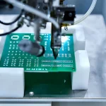
<img src="https://www.gopcba.com/wp-content/uploads/2020/12/project_image_07.jpg" alt="Bare circuit board being scanned to capture copper layer artwork” />
Each copper layer is then captured separately, and the board must be positioned square to the scanning axis. A rotated image cannot be aligned or scaled reliably afterwards, and no amount of subsequent processing will recover the geometry. Capturing at higher resolution than the finished feature size demands is another precaution that costs nothing at this stage and prevents a repeat later.
From Image to Vector Data
The captured image is adjusted for contrast and brightness until copper and non-copper areas are clearly distinguished, then converted to a two-level image. The result is inspected for continuity: where a line is broken or blurred, the process has to be repeated rather than manually repaired, because hand corrections tend to hide systematic capture problems.
The cleaned images are then imported into a layout tool as a background reference, and the copper layer is traced manually on top of them. This is the labour-intensive part of reverse engineering, and it is the point at which most of the accuracy of the final result is determined. The traced layer is checked against the artwork before the reference image is discarded.
Rebuilding the Netlist and Checking It
The copper layer defines connectivity, so once the layers exist a netlist can be extracted and compared with the physical board. Continuity checks between the pads that should be connected, and isolation checks between those that should not, catch tracing errors that are invisible on screen.
The schematic is then reconstructed from the netlist and the component record. Where the design is complex, reproducing the original drawing style is unnecessary; what matters is that the connectivity, the component values and the net names are right. If the rebuilt board is to be manufactured, the design also has to be brought into compliance with current fabrication rules, which the original may well violate.
Multilayer Boards and Registration Problems
Multilayer construction raises the difficulty sharply. Inner layers cannot be imaged until they are exposed, which means destructive preparation, and each layer has to be captured with the same positional reference so that the layers can be aligned afterwards.
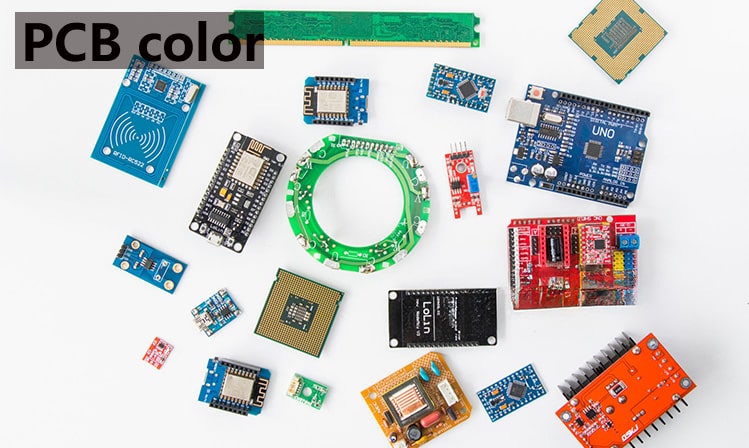
Registration is the recurring failure. Alignment error creeps in during capture and again during tracing, and it accumulates until pads no longer line up between layers. Plated and non-plated holes are especially easy to confuse, because both appear as openings in the copper and only the barrel plating distinguishes them. Extra care in the early stages pays for itself here, since a misregistration discovered at the end invalidates the work on every layer.
Limits, Ethics and Verification
Reverse engineering has real limits. Internal planes with continuous copper, embedded components and controlled impedance structures are difficult to characterise from the outside, and material properties cannot be measured from a finished board at all. Where performance depends on those factors, reconstruction is approximate.
It also has legal and ethical boundaries. Reproducing a design for study, for repair support or for interoperability is generally different from copying it for commercial advantage, and the distinction should be settled before work begins. Whatever the purpose, the finished data should be verified against the original by comparing critical dimensions, checking connectivity and, where feasible, producing a prototype that is functionally tested alongside the source board.
Working Efficiently on a Large Board
Scale changes the economics. A small two layer board can be reconstructed in an afternoon, while a dense multilayer assembly may take weeks of tracing, and the labour is the dominant cost. Planning the work matters more than working quickly, because a technique that saves an hour early can invalidate a week of effort later.
The practical approach is to divide the board into functional blocks and complete one block at a time, checking each against the physical board before moving on. Tracing an entire layer and then looking for mistakes is slower than verifying as you go, because errors found late are surrounded by dependent work. Naming conventions for nets and components should be fixed at the start, otherwise the netlist becomes unreadable before the work is half finished.
Tooling helps as well. Using the captured images as a background layer with grid snapping and a consistent grid origin removes most of the small positional errors that accumulate during manual tracing. Where the design must ultimately be manufactured, the reconstructed data should be checked against current process rules rather than the rules of the era it came from, since the original may use clearances that no longer exist in production. Constraints on multilayer construction are described in multilayer PCB manufacturing challenges, and the dimensional behaviour that drives registration requirements in PCB dimensional stability and expansion. Mechanical details such as mounting features, which are frequently undocumented in old designs, are covered under board outline and mounting design.
FAQ
Can every board be reverse engineered? No. Simple single and double sided boards can be reconstructed accurately, but boards with continuous internal planes, embedded components or critical impedance requirements can only be approximated.
Why does the scanning step matter so much? The captured image is the only positional reference for everything that follows. A skewed or low resolution scan cannot be corrected later, and its error propagates into every layer that is traced from it.
Why are plated and non-plated holes easy to confuse? Both appear as openings in the copper artwork, and only the plated barrel connects layers. Distinguishing them requires checking the physical board rather than the image.