Face Recognition PCB Design: Camera, Processor and Thermal
A face recognition device has to capture an image, process it with a neural network and return a decision, all within a fraction of a second and inside a small enclosure that is often mounted on a wall in direct sunlight. The circuit is a vision system with a hard real time requirement, and a face recognition PCB is designed around the two constraints that dominate it: image quality and heat.
What the Device Does
A camera captures a frame through an infrared or visible filter, an image signal processor conditions it, and a processor runs the recognition model. The result drives a lock, a display, a network interface or an access control system, and the device usually also manages a secure element and a communication link.
The processing load is bursty. Between recognitions the device may be almost idle, and during one it draws a large current for a short period. That profile is harder to manage than a steady load, both for the power delivery and for the thermal design.
Camera Interface and Image Quality
The image sensor connects through a MIPI differential serial interface requiring impedance control, length matching within each lane and a continuous reference plane. Because the camera is often a separate module on a short flex, the board’s job is to carry that interface without adding loss or jitter.
Image quality also depends on the supply to the sensor. Its analogue rails need filtering and a separate return path, and the clock that drives it must be clean, because jitter shows up as noise in the image and reduces the recognition rate. The layout approach is close to the one described for a mixed signal PCB, applied to a sensor rather than to a converter.
Infrared Illumination
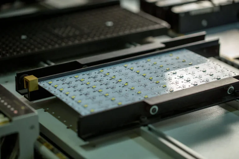
Most recognition systems illuminate the subject with infrared emitters so that the face is lit consistently regardless of ambient conditions. The emitters are driven in short pulses at high current, and that current is the largest transient on the board.
The driver belongs close to the emitters, with a short and wide current path and its own decoupling. Because the pulse is short, the supply has to provide the peak current locally rather than through a long trace to the regulator, and the return path for the emitter current should not share the sensor ground. Sizing the conductors uses the usual current and temperature calculation described in trace width and current calculation.
Processor Power Delivery
The recognition processor has several rails with different voltages and different sequencing requirements, and the core rail draws a large current that changes quickly with the computing load. Multi phase regulators and a large number of decoupling capacitors are typically required close to the device.
Capacitor placement matters more than the total value. The highest frequency decoupling needs to be within a few millimetres of the pins, with a low inductance connection to the power and ground planes. Where a reference design is supplied by the processor vendor, its layout should be followed closely, because the power delivery network is designed as a system and cannot be improvised. The general principles behind that work are described in multilayer PCB advantages for high speed.
Thermal Management
The processor runs its heaviest computation in bursts, and the device is often sealed with no airflow. Heat has to leave through the board and the enclosure, and the thermal design must keep the processor below its limit during sustained operation.
Copper area and thermal vias under the device are the standard measures. Where the enclosure permits, a thermal pad or a metal standoff conducts heat into the housing, which is the most effective path in a sealed product. Because the load is bursty, the thermal mass of the board and the housing also matters: a short burst can be absorbed, while a long sequence of recognitions will not. The verification should therefore run a realistic sequence rather than a single frame, and the temperature should be measured in the enclosure at the highest expected ambient.
Power Sequencing and Reset
The processor requires its rails to come up in a defined order and its resets to be released after the supplies are stable. Doing this wrongly produces a device that boots inconsistently, which is one of the more difficult faults to diagnose because it depends on the rise time of the supply.
A dedicated sequencing device or an integrated power management chip is the usual solution, and the sequencing order should be verified on the bench rather than assumed from the data sheet. The reset and boot configuration pins must be strapped correctly and, where a boot mode is selected by a resistor, the value should be checked at the extremes of the tolerance range.
Security and Data Protection
A device that stores biometric templates is a target, and the board carries features that support the security architecture: a secure element, an encrypted memory interface and, often, a tamper detection input that clears the keys if the enclosure is opened.
From a layout perspective, tamper detection needs a mesh or a set of traces that cannot be bypassed, and the secure element should be placed where it cannot be probed easily. These are cost and area decisions that have to be made early, because retrofitting a security feature into a finished layout is rarely practical.
Electromagnetic Compatibility
The board contains a high speed image interface, a fast processor and a pulsed infrared driver, all in a plastic enclosure with no shielding. Meeting emission limits requires attention to the switching loops and to the interfaces that leave the board.
Filtering at the external connectors, keeping the high current loops small, and providing a continuous return under the high speed lines are the primary measures. Where the network interface is wireless, the radio and the camera should be separated physically, with the antenna placed away from the processor and the display. The techniques are those described in EMI suppression design principles.
Mechanical and Optical Alignment
The camera has to be aligned with the aperture and with the infrared illuminators, and the alignment tolerance affects recognition performance. A board that warps moves the sensor and shifts the optical axis, so flatness is a functional parameter rather than a cosmetic one.
The sensor is usually mounted on the main board or on a small sub board fixed to the housing. Whichever approach is used, the mechanical datum should be defined on the drawing, and the mounting features should be designed so that the assembly is located by the datum rather than by the connector.
Reliability and Service Life
Access control devices run continuously for years, often in conditions that include dust, humidity and temperature cycling. The board should be designed with that in mind: compliant joints on large components, protection against moisture where it is exposed, and a thermal design that does not rely on margins that will disappear as dust accumulates.
Firmware and model updates also mean the device will be reflashed over its life, so a recovery path that cannot be bricked by a failed update is worth designing in. That is a system decision, but it affects the board through the boot configuration and the debug interface that must remain accessible.
FAQ
Does the camera need to be on a separate board? It is often on a small module connected by a flex, which allows the optics to align with the housing independently of the main board. The interface still has to be routed as a controlled impedance line.
Why does the device fail to boot occasionally? Almost always power sequencing or reset timing. Verifying the rail order and the reset release on the bench resolves it far faster than changing components.
How much thermal margin is needed? Enough that the processor stays below its limit at the highest ambient with the enclosure closed and with a realistic recognition workload, not with a single frame on an open bench.