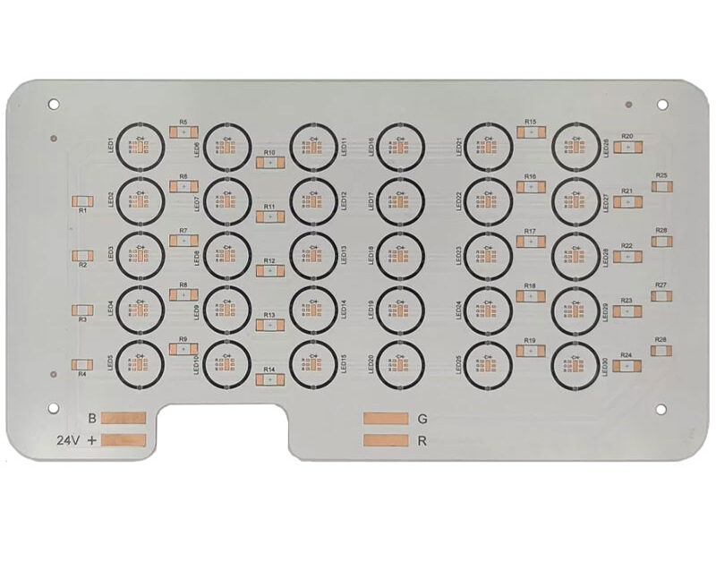
PCB Outer Layer Routing Design Rules for Manufacture
The outer layers of a board are the ones the fabricator sees first and the ones where the smallest mistake is the most expensive, because everything on them has already been paid for by the time the defect appears. Inner-layer design is judged by what can be laminated over; outer-layer design is judged by what survives etching, drilling, solder mask and profiling.
This article collects the outer layer routing rules that a layout has to satisfy before the data is released, covering the pad geometry around drilled holes, the minimum trace and space, the way copper is placed near machined edges, and the clearances that V-scoring and routing demand. The numbers are not arbitrary: each one exists because a machine, a chemical or a thermal cycle has a tolerance that the copper has to respect.
Why the Outer Layers Carry Extra Rules
An outer layer is exposed to every mechanical operation in the process. It is drilled, it is profiled by a router or a punch, it may be scored, and it carries the pads that solder has to wet. Each of those operations removes or stresses material close to the copper, so the copper has to stand back from the features that the machine will cut.
The consequence is a set of clearances that do not appear in an electrical rule set. A trace that is perfectly acceptable in the middle of the board becomes a defect when it sits too close to the profile line, because the registration tolerance of the profiling step is added to the registration tolerance of the imaging step.
Annular Ring on Plated Holes and Vias
Every plated hole needs a ring of copper around it that survives the drill tolerance. The ring has to exceed the drilled diameter by a defined amount on each side, because the drill can wander within its tolerance and the copper can be pulled back by etching. A ring that is too thin on one side is either an open or a reliability risk, depending on how much of it is left.
The rule that follows is a minimum pad diameter and a minimum hole diameter, both of which are usually expressed in the same units as the drill table. Vias also need an outer diameter that leaves enough copper for a via to be counted as a reliable connection, and the pad must be large enough that the drill can hit its target without eating into the ring. The rules that govern via geometry are the natural companion to the ring rule here.
Minimum Trace Width and Spacing
The minimum width and the minimum gap on an outer layer are set by the etching process rather than by the current the trace carries. Thin copper etches faster than thick copper, and the sides of a trace are attacked as well as the top, so a design that pushes the width and the spacing to the process limit will see a spread of results across the panel rather than a single result.
Hole-to-hole spacing deserves equal attention, because two holes that are close together leave a narrow web of laminate between them that can crack during drilling or snap during assembly. The rule is normally expressed as a minimum centre-to-centre distance or a minimum web, and it applies to vias placed inside a thermal pad as much as to a row of connector pins.

The Copper Grid and Solid Floods
Large areas of copper are often drawn as a grid rather than a solid pour. The reason is mechanical: a solid sheet bonded over a large area traps volatiles and heat, and the difference in expansion between the laminate and the copper can lift the foil during soldering. A grid gives the same electrical function with less area bonded, and it lets the board breathe.
The grid still has a rule of its own. The openings have to be small enough not to swallow the geometry of the pour, and the strands have to be wide enough to survive etching, which sets a minimum strand width and a minimum spacing between strands. Where a solid pour is chosen for thermal reasons, the trade-off between heat spreading and board flatness needs to be decided deliberately, and the comparison of mesh and solid flooding is the place to make it.
Etched Legend and Silk Screen
Text can be produced on the outer layer in two ways, and they have different limits. Legend printed with solder mask ink can be small and crisp, while text etched into the copper has to be much wider, because the etchant will eat into thin lines from both sides and a character that is too fine will simply disappear.
Identification marks that have to survive, such as polarity marks, pin one indicators and board part numbers, are therefore usually etched rather than printed, and their stroke width has to be generous. Marks that only help during assembly, such as reference designators, can be printed, but they still have to sit clear of pads and of any area where solder will flow.
Clearance Around Non-Plated Holes and Edges
A hole that is not plated still removes material, and the copper around it has to stand back far enough that the drill, which is guided but not perfect, does not clip the trace beside it. The same logic applies to copper that runs near the board edge: the material that will be removed by profiling is not available as a safety margin, because the profile line moves within its own tolerance.
Slots are the difficult case, because they combine a machined edge with a shape that may run past several layers of circuitry. Copper has to stand back from a slot on every layer it passes through, and the shape itself has to be drawn as a closed contour that the router can follow. The specific distances belong with the general slot and edge routing rules, and they should be applied to the slot walls rather than only to the board outline.
<img src="https://www.gopcba.com/wp-content/uploads/2026/05/Industrial-IOT.jpg" alt="Copper clearance from a V-CUT score line” />
Router, Punch and V-CUT Clearances
A routed edge and a punched edge have different tolerances, so they carry different clearances. A board that will be routed with a cutter calls for copper to be held further back from the profile line than a design that happens to be routed in the prototype shop but punched in volume, because a punch die removes material in a single stroke with a tolerance that is set by the tool rather than by a program.
V-scoring adds a third case, and its clearance depends on board thickness. Thicknesses around 1.6 mm call for roughly 0.8 mm from the copper to the score line, a 1.2 mm board about 0.7 mm, boards between 0.8 and 1.0 mm about 0.6 mm, and thinner boards about 0.5 mm. Gold-finger edges need more, around 1.2 mm. These distances are measured to the scoring line, and they apply on both sides of the panel.
What to Put on the Fabrication Drawing
The outer layer rules are only useful if the fabricator can see which ones apply. A drawing that states the stack-up, the finished thickness, the copper weight, the profile method and the location of any scoring is far more useful than a note that refers to a general standard, because the clearances and the tolerances are chosen from those facts.
The panel is the last consideration. Where several boards share one panel, the spacing between them and the rails at the edge are chosen by the fabricator, but the copper clearances around each board outline still come from the design. The broader requirements for the outline and mounting features cover the mechanical side of the same discussion.
FAQ
Why is the annular ring treated separately from the trace width? Because it is produced by two different tolerances working against each other, drill registration and etch pull-back, while a trace is produced by one imaging step.
Can a board be routed after it has been scored? Yes, but the scoring line is a stress raiser, so copper and components have to be kept clear of it on both sides, and the break-out direction should be defined.
Do these rules change with copper weight? They do. Heavier copper etches with more sidewall attack and requires wider minimum features, so a design that moves from one ounce to two ounce copper should have its minimums reviewed.