High Frequency PCB Manufacturing: Material and Process Control
A high frequency PCB is not a board made from a different kind of circuit. It is an ordinary circuit built on a laminate whose electrical properties stay predictable at the frequencies where the signal travels as a wave rather than as a current in a wire. That distinction drives everything about how the board is processed, from the way the material is cut to the way the holes are made conductive and the way the solder mask is cured.
What Counts as a High Frequency Board
The line is a matter of convention rather than a physical threshold. The label is generally applied above roughly 300 megahertz, or where the wavelength falls below about a metre, and materials are described as microwave grade above about three gigahertz, or a wavelength below 0.1 metre. In practice most fabricators treat anything operating above about one gigahertz as a high frequency board, because that is where the loss and the dimensional sensitivity of ordinary FR-4 stop being acceptable.
Applications follow the frequency. Mobile communication products, power amplifiers and low noise amplifiers, passive devices such as splitters, couplers, duplexers and filters, and automotive radar, satellite and radio systems all sit in this band. The direction of the industry is towards higher frequency rather than lower, which makes the material and process choices permanent rather than temporary.
Laminate Families
Two families cover most work. The first is ceramic-filled thermoset material, which processes much like FR-4 with the same general flow, but is brittle and prone to cracking, so drill and router life drops by around twenty percent. Grades in this family include the Rogers 4350B and 4003C, the Arlon 25N and 25FR, and the Taconic TLG series.
The second is PTFE, which offers the lowest loss and the most demanding processing. Grades include the Rogers RO3000, RT and TMM series, the Arlon AD, AR, IsoClad and CuClad series, the Taconic RF, TLX and TLY series, and the F4B, F4BM, F4BK and TP-2 materials. The dielectric constant of the chosen grade sets the geometry of every controlled impedance trace on the board, and it moves with frequency and temperature, which is why the material has to be fixed before the stack-up is designed.
Cutting and Drilling PTFE
Cutting has one rule that overrides everything else: the protective film stays on the material. PTFE is soft and marks easily, and a scratch or a compression mark in the surface is a permanent change in the dielectric. It will not be visible in the finished board, but it will be measurable in its performance. Handling discipline from the cutting stage onwards is part of the process, not a courtesy.
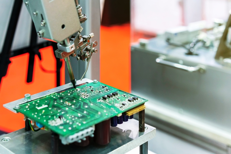
Drilling is where the difference from FR-4 shows most clearly. A new drill bit is used, a single panel per stack is preferred, and the foot pressure is set around 40 psi. Aluminium is used as the entry material and a one millimetre melamine board as the backing, with the stack clamped firmly. The hole is cleared of dust with an air gun after drilling. Parameters follow the usual logic – a smaller hole calls for a higher spindle speed, a lower chip load and a slower retract – and the machine chosen should be the most stable one available, because PTFE deflects rather than cutting cleanly when the setup is not rigid.
Hole Activation Before Plating
A hole in PTFE does not accept electroless copper the way a hole in FR-4 does. The surface has to be activated first, and two routes are used: plasma treatment, or a sodium naphthalene activation that chemically modifies the surface. Either way the purpose is the same, which is to give the subsequent plating something to bond to.
From there the plating sequence is conventional, with tighter control on the etch. The micro-etch is held to about twenty microinches of removal, and the panel enters the plating line at the de-grease stage. Where a second pass through plating is needed, the panel re-enters at the appropriate stage rather than running the whole sequence again. The difficulty that appears most often is copper adhesion on the hole wall, because a PTFE surface that has been inadequately activated will plate and then delaminate under thermal stress rather than failing immediately.
Imaging, Etching and Solder Mask
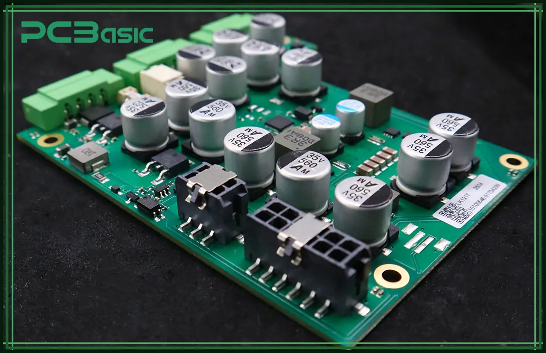
Imaging and etching on a high frequency board are judged by different criteria than on a standard board. Line width has to hold to the tolerance the impedance target requires, and defects that are cosmetic elsewhere are electrical here: a notch in a trace, a pinhole in the copper, or a width that drifts along the run all change the local impedance. Etch control and inspection after etch are therefore tighter than the FR-4 norm.
Solder mask is the step that surprises people. The surface is prepared with an acid wash rather than a mechanical scrub, because abrading this material damages it. The panel is then baked at around 90 degrees Celsius for 30 minutes before the mask is applied, and the cure runs in three stages at 80, 100 and 150 degrees Celsius, each for about 30 minutes. Adhesion is the recurring problem. A masked panel showing the mask lifting from the base material can be reworked by stripping it, re-activating the surface and starting again, and blistering and poor adhesion are among the most common process difficulties on this material.
Routing and Handling
Routing follows the same logic as drilling. The panel is supported on both sides, typically with paper against the circuit face and copper-free FR-4 or phenolic backing above and below, and clamped so that the material cannot flex into the cutter. After routing, the burrs along the edge are removed by hand with care, because the same softness that makes the material mark easily makes the edge easy to damage while cleaning it.
The finished panel is separated with sulphur-free paper and inspected visually. Throughout, the objective is to keep both the copper surface and the base material free of scratches, dents and contamination, because on this material a handling defect is a dielectric defect. The overall expectations for a finished board of any type are described in PCB design quality characteristics, and the routing discipline that keeps impedance predictable along the trace is covered in high frequency traces and data bus routing. Where the design will be built as a multilayer stack, the points to agree with the fabricator in advance are set out in multilayer PCB prototype requirements.
FAQ
Is every board above one gigahertz made from PTFE? No. Ceramic-filled thermoset laminates cover much of the range and process more like FR-4. PTFE is chosen where loss has to be minimised, and it costs more to process.
Why does drill life drop on these materials? Because they are abrasive and brittle. On ceramic-filled grades drill and router life falls by roughly twenty percent; on PTFE the softness demands a rigid setup and a fresh bit.
Why is the solder mask cured in three stages? So that solvent leaves the film gradually. A staged cure at 80, 100 and 150 degrees Celsius avoids trapping solvent, which is what causes blistering and poor adhesion.
Can a scratched high frequency board be saved? Usually not. A mark in the surface changes the dielectric locally, and once the board is processed the damage is buried. Handling discipline is the only real control.