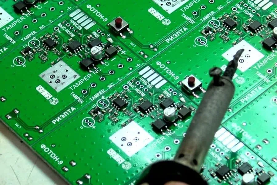
Pad Design Criteria for Reliable Solder Joints
A pad is the only place where the board and the component are physically joined, and it is sized and shaped by a set of rules that are less about the electrical design than about the soldering process. A pad that is too small starves the joint; a pad that is too large wastes space and makes bridging more likely; a pad on a copper pour that is not thermally relieved is difficult to solder at all. The criteria below cover the geometry that matters.
Pad Shape and Size
The starting point is the standard footprint library, because a pad that has been used successfully on other products is a pad that has already been validated. Beyond that, three limits govern the geometry. The annular ring on any pad should be at least 0.25 millimetres on one side, the overall pad diameter should not exceed three times the hole diameter, and the gap between the edges of two adjacent pads should be greater than 0.4 millimetres wherever the routing allows it.
Shape follows the same reasoning. Where the routing is dense, an oval or elongated pad keeps the solderable area while reducing the space the pad occupies. On a single sided board the pad diameter or minimum width is typically 1.6 millimetres, while a low voltage pad on a double sided board needs only the hole diameter plus 0.5 millimetres, because an oversized pad invites bridging without adding anything to the joint. Where the hole exceeds 1.2 millimetres or the pad exceeds 3.0 millimetres, a diamond or plum blossom shape is used so that solder and thermal expansion are distributed rather than concentrated.
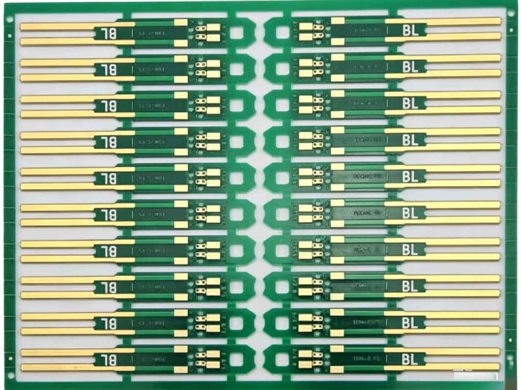
Spacing and Bridging
Bridging is the defect that pad geometry controls most directly. Two pads placed close together with a generous solder deposit will connect, and the risk rises with the length of the parallel edges and with the amount of solder present. Where the pad pitch falls below 0.4 millimetres, solder mask is usually extended between the pads to reduce the solder available, and where a row of four or more pads on the same axis is spaced that closely, an extra empty pad or an enlarged final pad at the end of the row gives the trailing solder somewhere to go during wave soldering.
The direction of the component relative to the solder wave also matters. A component whose long axis is parallel to the wave presents the minimum number of edges to the solder at once, and where the axis is perpendicular a solder thief or an enlarged pad at the exit end absorbs the excess. These are process accommodations rather than electrical ones, and they are the reason pad geometry is best decided with the assembly process already known.
Thermal Relief on Copper Pours
A pad connected to a large area of copper is difficult to heat, because the copper conducts heat away as fast as the iron supplies it. On a board with a ground or power area larger than about 500 square millimetres, the pad is therefore connected through a thermal relief: a small number of narrow spokes rather than a solid connection, so that the pad heats enough to melt solder while remaining electrically connected. Where the design cannot accept the relief, the alternative is to break the pour into a window or into a mesh so that the local copper area is reduced.
This is the same problem whether the joint is soldered by hand or by wave, and the same reasoning applies to the heat a reflow profile has to deliver. The trade-off between a solid pour and a mesh is discussed in copper flooding: mesh or solid.
Through-Hole Pads and Teardrops
Through-hole pads carry a second requirement, which is that the foil must not tear where the trace leaves the pad. On a single sided board the pad is fully covered with copper foil so that the joint is supported on all sides. On a double sided board the minimum is a teardrop, a fillet of copper that widens the junction between the trace and the pad and spreads the mechanical load of the lead. Where the lead will be clinched, the pad is shaped to follow the direction of the clinch so that the solder fillet is complete at the bend.

The underlying principle is that a pad serves two masters. It has to give the solder enough area to form a reliable joint, and it has to do so without taking area from the routing or creating a bridge to its neighbour. Where those two requirements pull in opposite directions, the process the board will go through decides which one wins, which is why the same component can justify a different pad on a hand assembled board and on one that runs over a wave.
Test Points and Probing
A test point is a pad that exists to be probed rather than to be soldered. Where a surface mount component sits at the end of a net with no through-hole part attached, adding a test point keeps that net accessible to in-circuit test equipment, and its diameter should be at least 1.8 millimetres so that a probe seats reliably. The same applies to the pads of a fine pitch device: where those pads are not connected to anything a probe can reach, a dedicated test pad is added, placed outside the silkscreen outline of the part rather than under it.
Overlap between test points and neighbouring features is worth checking on the finished layout. A test point that a probe cannot reach because of a tall component beside it is a test point that does not exist, and discovering that at the test stage means the net is untested rather than failing.
Solder Mask Details
Solder mask is part of the pad design rather than a decorative layer. The openings have to be large enough that the mask does not encroach on the solderable area and small enough that the web between two fine pitch pads does not lift. Where the pitch is tight, the web is defined by process capability rather than by the drawing, and the fabricator may ask for the opening to be adjusted to suit. The ink itself has a working window: its thixotropy, the property that lets it hold a printed edge and then flow, determines how cleanly the web forms. That behaviour is described in solder mask ink thixotropy.
The finish on the exposed pad is the last variable. A joint that must be reliable over a long service life benefits from a finish that resists oxidation and wets consistently, and the comparison between the common options is set out in lead-free versus leaded solder.
FAQ
How small can a pad annular ring be? A minimum of 0.25 millimetres on one side is the usual floor, and the pad diameter as a whole should stay below three times the hole diameter. Below that the risk of breakout rises sharply.
Why does a pad need a thermal relief? Because a pad connected to a large copper area cannot be heated enough to melt solder. Narrow spokes in place of a solid connection let the pad reach temperature while keeping it electrically connected.
How large should a test point be? At least 1.8 millimetres in diameter, so that in-circuit test probes seat reliably. On fine pitch devices the test pad is placed outside the silkscreen outline of the part.
What stops solder bridging between pads? Spacing, the solder mask web between the pads, and the direction the component presents to the solder wave. Where pads are closer than 0.4 millimetres the mask does most of the work.