Five-Order Blind Via HDI Boards: Process Flow and Control
A five-order blind via board is the point at which high density interconnect stops being a variation on conventional multilayer fabrication and becomes a separate discipline. Each order of blind via adds one more sequential lamination cycle, one more laser drilling step and one more layer to layer registration event, and the yield of the finished board is roughly the product of the yields of all those steps. Understanding the process flow is therefore the first step towards designing a stack-up that can actually be built.
The term order counts how many times a via spans only part of the layer stack. A first order blind via connects the outer layer to the next one down. A second order via spans two layers, and a via that spans three layers is third order. When the same board also contains a via that reaches from the other side, the count is expressed for each side separately, so a five-order construction means five successive lamination and drilling cycles on one face.
Why Build-Up Goes This Far
The driver is escape routing density. Fine pitch ball grid array packages with pitches below 0.5 mm leave too little room between pads for the number of through vias that a conventional stack would need, and through vias also occupy space on every layer they pass. Blind and buried vias remove those blockages, so the same routing can be completed in fewer layers or with shorter stubs. Short stubs matter as much as density, because a through via stub behaves like a transmission line stub that degrades the channel at high data rates, an effect discussed in the back drilling design notes.
A five-order stack is normally an any layer construction in which every layer pair can be connected directly. The advantage is total freedom in the vertical direction; the cost is that the board passes through the plating and lamination line five times, and every pass adds risk of misregistration, resin flow defects and dimensional growth. Designs that genuinely need five orders are rare, and a careful review often finds that a lower order with a better fanout achieves the same result, which is why any layer HDI decisions should be made with the package and the router in the room.
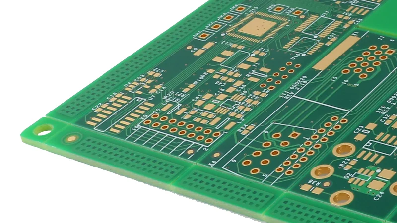
Sequential Lamination Flow
The core of the process is build-up lamination. The fabricator starts with a rigid core, drills and plates it conventionally, then laminates a dielectric film or a resin coated copper foil onto each face. A window is opened in the copper of the newly added layer, the dielectric is ablated with a laser, and the resulting microvia is plated and planarised. The board is now a one order build-up, and the same cycle is repeated to reach the required order.
Each cycle imposes a thermal excursion on the layers already completed. Thermoset resin continues to cure, the copper expands and the substrate shrinks slightly on cooling, so layer-to-layer registration drifts as the order increases. Fabricators counter this with compensation in the artwork, with low shrink factor materials, and by measuring actual dimensional movement after each cycle rather than relying on a single global scale factor. The material property that governs most of this behaviour is the coefficient of thermal expansion, which is why low loss laminate selection and CTE are assessed together when a high order stack is proposed.
Laser Drilling the Microvias
Microvias are formed with lasers because mechanical drilling cannot produce reliable holes below roughly 0.15 mm in these dielectrics. Carbon dioxide lasers cut resin and glass efficiently but reflect from copper, and ultraviolet lasers cut copper cleanly but remove less material per pulse. The composite approach uses a UV beam to open a copper window and a carbon dioxide beam to remove the dielectric beneath it, which gives a controlled taper and a clean bottom target pad.
The critical parameters are energy density, pulse overlap and the depth to which the copper window is opened. Too much energy produces a barrel shaped hole with a neck that is difficult to plate, and too little leaves resin smear on the target pad that shows up later as a high resistance via or an intermittent open. The target pad is also the registration reference, so the same pad must survive four previous lamination cycles without oxidation, which is why surface preparation before each drilling step is a process control item.
Plating and Void Free Fill
Filling a microvia without a void is harder than plating a through hole, because the via is short and wide and the electrolyte cannot flow through it. Panel plating alone tends to close the mouth of the hole and trap chemistry inside, so acid copper plating is usually combined with a pulse or periodic reverse waveform that alternately deposits and dissolves, improving throwing power at the via bottom. Where the via sits directly on a pad that must carry a component, the hole is filled with a conductive or non conductive paste and then capped with copper, a sequence described under copper plating via filling.
Voiding is verified by cross section on a coupon that is laminated with the production panel and drilled with the same recipe. A cross section at the end of the first production lot is the cheapest possible confirmation that the fill process is under control, and it should be repeated when the dielectric supplier, the paste batch or the laser recipe changes. Voids that are not detected at this stage become intermittent opens after thermal cycling in the field.
Registration, Inspection and Yield
With five build-up cycles the accumulated registration error becomes the dominant yield factor. Fabricators use separate targets for each build-up layer, measure the actual offset after lamination and apply a per panel correction, which keeps layer-to-layer registration inside the microvia capture pad, and they inspect with automated optical equipment after each drilling step so that a drift is caught before another layer is added on top. Once a subsequent layer covers a misregistered microvia, the defect is invisible to optical inspection and can only be found by electrical test or cross section.
Reliability is assessed with thermal cycling between the glass transition temperature limits, with high temperature storage and with a reflow simulation at the temperatures the assembly will actually see. Interconnect stress test coupons give a quantitative measure of the number of cycles to failure for the via chain, and the results should be compared against the field life the product needs. For a board with this much invested in it, the high density interconnect qualification data is as important as the electrical design.
FAQ
When is a five-order blind via stack actually necessary? Usually only when the package pitch is below 0.4 mm and the router cannot escape the inner rows with a lower order build-up. Most designs that appear to need five orders can be solved with a thinner core, a different fanout or a changed ball assignment.
Is an any layer stack the same thing? They overlap but are not identical. An any layer board uses the same build-up process on both faces and allows a via between any two adjacent layers; the order count is one way of describing how many of those layers are stacked on each side.
What is the most common cause of low yield? Accumulated layer to layer misregistration, followed by resin voiding in the microvia fill. Both are process control problems rather than design problems, which is why the fabricator should be involved before the stack-up is frozen.