10 Layer HDI Stackup: Microvias, Stacked Vias and Design Rules
Ten layers is where a board stops being a stackup and becomes an architecture. At that layer count the connection between the layers is no longer a detail of the routing but the thing that determines how many lamination cycles the fabricator must run, how the panel is built, what yield can be expected and how much the board costs. A 10 layer HDI design is therefore planned from the via structure downwards.
What Ten Layers of HDI Mean
A conventional ten layer board is laminated once, drilled through and plated. An HDI board of the same layer count uses microvias, formed by laser, that connect only the outer layers to the first inner layer, and deeper connections made either by stacked structures or by additional lamination cycles. The core of the board is built first with buried vias, and the outer layers are added as build-up layers on top of it.
The reason for the complexity is escape routing. A fine pitch device may have a pad pitch below half a millimetre, and the space between pads cannot accommodate a through via and its clearance. Routing the signal only as far as the first inner layer, and then continuing on a layer that has room, is what makes the device usable, and the microvia is what makes that possible.

Stackup Architectures
Most ten layer HDI boards are built around a rigid core with build-up layers on one or both faces. A symmetric arrangement keeps the board flat through the lamination cycles, which matters because each cycle applies heat and pressure and a stack that is unbalanced will bow. The layer assignment should place the ground planes adjacent to the layers that carry the fastest signals and keep the power distribution spread over more than one plane pair.
The number of build-up layers on each side is chosen together with the via structure. One build-up layer per side is enough for a simple microvia escape; two or three per side are needed when the routing has to move between several layers near the surface. Each additional build-up layer is another lamination cycle, and the cost rises faster than the layer count suggests.
Microvia Structures
A staggered microvia lands on a pad on the layer below, and the next via starts from that pad and goes down one more layer. A stacked microvia places the second via directly on top of the first, so the two form a single vertical connection. A skip via reaches two layers in one step. Each of these has a different cost and a different reliability profile.
Stacking is the most space efficient and the most demanding. The via below must be completely filled and plated flat, or the next laser via will be drilled into a void. That requirement is what makes via filling a process of its own, and it is why a stacked structure costs more than a staggered one of the same layer count. The structures and their implications are described in blind and buried via stack selection.
Sequential Lamination Cycles
Each build-up step is a lamination cycle: the core is drilled, plated and filled, a dielectric layer and copper foil are added, the microvias for that level are drilled and plated, and the surface is planarised before the next level begins. A typical 10 layer HDI board therefore requires two or three cycles in addition to the initial core lamination.
Cycle count drives yield and lead time more than any other decision. Every additional press is an opportunity for misregistration, resin starvation or a void, and a board that fails at the last cycle loses all the work invested in the earlier ones. Keeping the number of cycles to the minimum that the routing requires is the single largest cost decision in the design, and the arrangement of a simpler stack is described in layer stackup for one to eight layers.
Via in Pad and Filling
On a dense HDI board the microvia frequently ends inside a component pad, because there is no room to place it beside the pad and route out. A via in pad must be filled and capped so that the surface is flat enough for solder paste to print correctly, and so that the paste does not wick into the hole during reflow and leave a void in the joint.
Copper filling is used where the via has to carry current or where a stacked via will be built on top; resin filling with a plated cap is used where flatness is the requirement. Either way the fill quality is verified on samples, because a partially filled via is invisible from the surface until it causes a defect. The comparison between the options is set out in via in pad or plated through.
Design Rules for a Ten Layer HDI Board
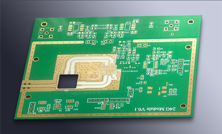
The rules are tighter in every dimension. Microvia diameter is limited by the laser and by the dielectric thickness, with the aspect ratio of a laser via generally kept near one to one because a deeper hole cannot be plated reliably. Land diameter, capture pad size and the registration tolerance between layers all become critical, because a microvia that misses its target pad by a few tens of micrometres breaks the connection.
The design should leave the largest capture pad the routing allows on every microvia landing, keep the number of via levels as small as possible, and avoid mixing via types in a way that forces an extra cycle. Copper balance matters more than on a simple board because the stack is pressed several times, and the design rules a fabricator can hold should be requested before the stackup is fixed rather than discovered at the quotation stage.
What HDI Buys Electrically
The electrical benefit is short connections. A microvia is a fraction of the length of a through via and has correspondingly lower inductance and capacitance, so the impedance discontinuity at the transition is smaller and the stub that would resonate at high frequency does not exist. That is why HDI is used for the fastest interfaces even when the layer count could be lower.
The reference structure benefits as well. With more layers available, a signal layer can be placed next to a continuous ground plane instead of being routed over a fragmented one. The design of the transmission lines themselves does not change, and the options are described in microstrip and stripline routing.
Yield, Inspection and Cost
Yield on a ten layer HDI board is lower than on a conventional board of the same size, and the loss is concentrated in the later cycles. Inspection is correspondingly heavier: automated optical inspection on each build-up level, X-ray to confirm via fill and registration, microsection to measure plating thickness and via geometry, and electrical test on the finished board.
The cost drivers follow from the same list. The number of lamination cycles, the via structure, the material, the finish and the panel utilisation each contribute, and they interact: a design that needs stacked microvias throughout will cost more than one that stacks only where the escape routing demands it. Reducing the requirement to what the circuit actually needs is the most effective cost control available at the design stage.
FAQ
How many lamination cycles does a 10 layer HDI board need? Typically two or three in addition to the core lamination, depending on the number of build-up layers on each side and the via structure.
Can a 10 layer board be built without HDI? Yes, if the pitch allows a through via with adequate clearance. HDI becomes necessary when the escape routing of a fine pitch device requires it.
Why must a microvia be filled before stacking? Because the next laser via is drilled into the same position. A void in the fill traps chemistry and creates a defect that only appears later.