Telecom PCB Design: Backplanes, Speed and Reliability
Telecom equipment is built to run continuously for a decade in a rack that is never switched off, and its boards reflect that. The channels are long, the data rates are high, the power density is significant and the equipment is expected to keep working while cards are replaced around it. A telecom PCB is therefore designed for the worst case at the end of life rather than the best case at the start.
What the Equipment Requires
Three properties dominate. The board must carry high speed signals over distances that are long compared with consumer electronics, it must distribute power to many devices without an excessive voltage drop or temperature rise, and it must do both without interruption for years. Those requirements are met by material selection, by stackup design and by a great deal of verification.
Availability is a design input rather than an operational matter. A rack mounted system is typically built with redundant power, hot swappable cards and a backplane that carries the traffic between them, so the board has to tolerate a card being removed and inserted while the system is live, including the inrush current and the transient that follows.

Backplanes and Card Interconnect
A backplane is a large board whose job is to connect the cards. It may be many layers thick, it carries connectors for every slot, and its channels are long enough that loss and crosstalk become the limiting factors rather than the driver capability. The design of the channel, including the connector transitions at each end, is usually simulated before the layout is committed.
The connector is part of the channel. Its pin assignment determines how the signals can be routed away from it, and its ground pins determine the return path for the high speed pairs. Keying, guide pins and the mechanical engagement of the card are also designed into the board, because a backplane that is damaged during a card insertion is an expensive failure. The routing rules for the pairs are described in high frequency trace and data bus routing.
High Speed Channel Design
Long channels lose signal through the dielectric and through the copper, and they distort the edges as the higher frequencies are attenuated more than the lower ones. The answer is a low loss laminate on the layers that carry the fastest signals, a stackup that keeps those signals next to a continuous reference, and careful control of every via along the route.
Via stubs are a particular problem on a thick backplane, because a stub a few millimetres long resonates within the band of interest. Back drilling, blind vias or a redesign of the layer assignment can all remove the problem, and the choice between them depends on the stack and on the fabricator. The transmission structures themselves are described in microstrip and stripline routing.
Power Distribution
A telecom board may carry tens or hundreds of amperes at a low voltage, distributed to many devices. The distribution network has to deliver that current with a voltage drop and a ripple that the devices can tolerate, which means several plane pairs, heavy copper where the current is concentrated, and a large number of decoupling capacitors distributed across the board rather than gathered in one place. The plane structure and the placement of the bulk capacitance are therefore decided together rather than one after the other.
The thermal consequence follows. A converter that is eighty eight percent efficient produces twelve watts of heat for every hundred it delivers, and that heat has to leave the board. Where air cooling is used the airflow path must be unobstructed, and where conduction cooling is used the board must transfer heat into a cold wall through its mounting. The layout of the converters themselves is described in DC to DC converter layout and routing.
Reliability and Continuous Operation
The board has to survive ten years of thermal cycling without a cracked joint, which places constraints on the via structures, on the solder alloys and on the components chosen. It also has to tolerate the transients that occur when a card is inserted or removed, which is a layout question as much as a circuit one: the inrush path should be as short as possible and separated from the sensitive circuits.
Redundancy is designed at the system level but it imposes requirements on the board. Where two supplies are combined, the combining circuit must fail in a way that preserves the path, and the board must be able to operate with one side removed. Monitoring and reporting are part of the same design, so that the system knows a card is about to fail before it does. That requirement reaches the board as a need for stable reference voltages, for measurement points that can be probed in service and for a layout in which a single component failure does not take the whole rail down. Designing the monitoring path with the same care as the signal path costs little at the layout stage and is what makes an unattended rack maintainable.
Stackup and Material Choice
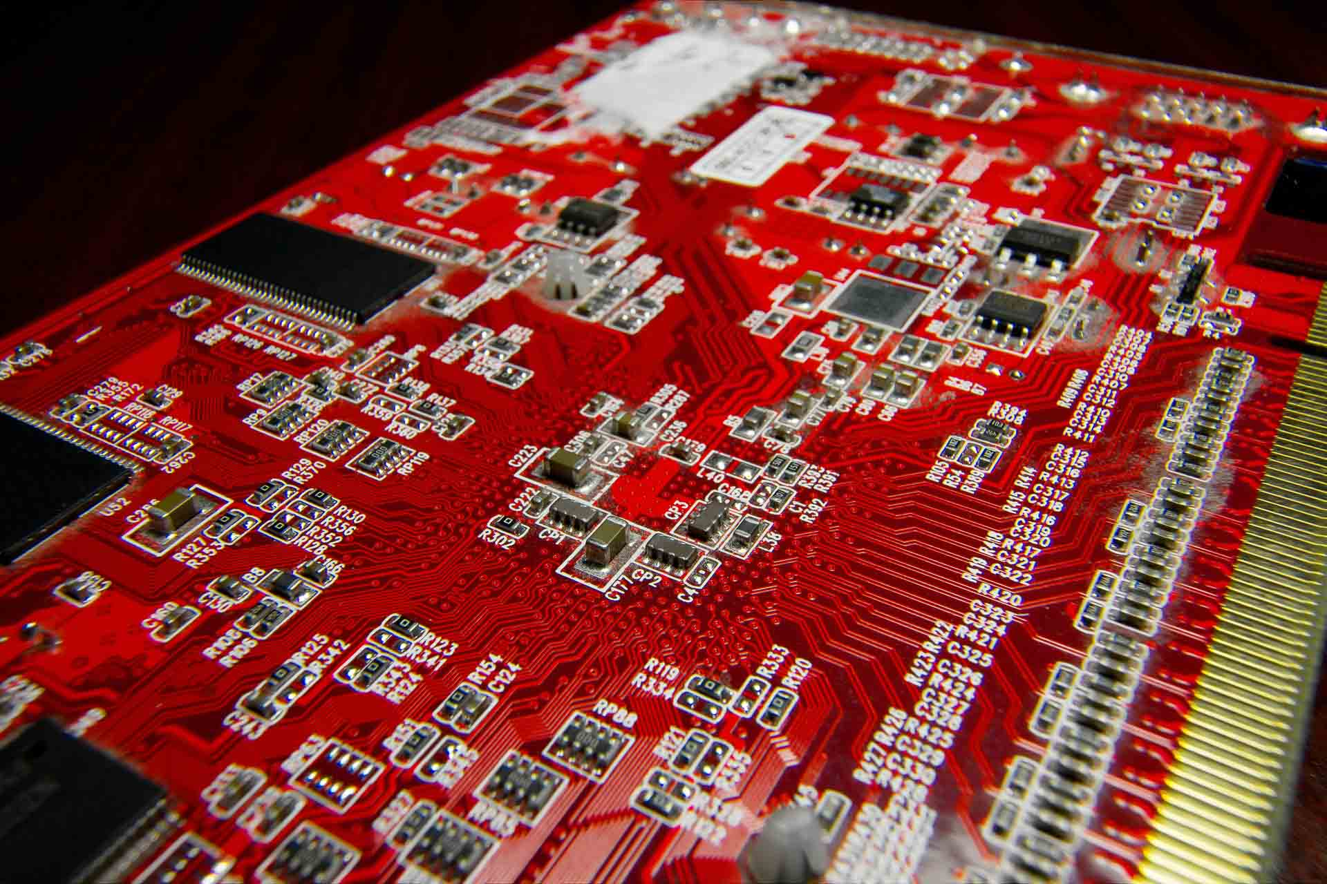
A telecom board is usually a thick multilayer stack, and the arrangement of layers determines both the electrical performance and the manufacturability. A symmetric stack keeps the board flat, several plane pairs provide the power distribution, and the signal layers are placed next to reference planes rather than next to each other. The general principles are set out in layer stackup for one to eight layers.
Material selection follows the channel lengths. Standard and high transition temperature epoxy glass is adequate for the control and power sections, while the longest and fastest channels use a lower loss laminate. A hybrid stack that uses the expensive material only where it is needed is the usual compromise, and it requires the two materials to be pressed together in one cycle.
Testing and Compliance
Verification covers three areas: the electrical performance of the channels, the integrity of the power distribution and the reliability of the assembly. Channel performance is measured with time domain reflectometry and with a vector network analyser on test structures, power integrity is verified by measuring ripple and droop under load, and reliability is verified by thermal cycling and by the qualification tests that the equipment has to pass.
Compliance testing then follows the product rather than the board, with emission and immunity tests performed on the finished equipment. Where a board fails those tests, the cause is usually a return path that is not continuous under a connector or under a fast interface, and the fix is normally in the layout rather than in the filtering.
FAQ
Does a telecom board need a special laminate? The fastest and longest channels do. Control, management and power sections are normally built on standard or high transition temperature epoxy glass.
Why is back drilling common on backplanes? Because the stub of a long through via resonates in the band of interest and degrades the channel. Removing the unused part of the barrel restores the performance.
How is hot swap handled on the board? With a controlled inrush path at the connector and a layout that keeps the insertion transient away from the sensitive circuits, together with monitoring that reports the event.