PCB Etching Process: Chemistry, Equipment and Control
Etching is the step that turns a copper covered panel into a circuit. Resist defines the pattern, and the etchant removes everything the resist does not protect. It sounds simple, and in principle it is, but the practical difficulty is that etching proceeds sideways as well as downwards. Controlling that lateral attack is what determines whether a fine line pattern comes out to tolerance or turns into a batch of scrap.
What Etching Has to Remove
A double sided panel begins as a laminate clad on both sides with copper foil. After imaging, the resist pattern covers the conductors, and the exposed copper has to go completely, leaving clean dielectric between features with no residual copper bridging them. On inner layers the same process applies before lamination; on outer layers it happens once the plating and resist work is complete.
The requirement is therefore twofold: remove all unwanted copper, and remove as little of the wanted copper as possible. Those two goals pull against each other, which is why the etching station is judged by an etch factor rather than by a single removal rate.
Chemistries and How They Differ
Cupric chloride is the workhorse for inner layers and for many outer layer processes. It is regenerated continuously and produces a controllable, reasonably uniform etch. Alkaline ammonia etchants are widely used for outer layers because they tolerate the tin or tin-lead resist used as an etch mask, and they can be regenerated automatically by measuring the specific gravity and the ammonia content.
Ferric chloride appears mainly in lower volume and prototype environments, where its simplicity outweighs the cost of disposal and the difficulty of regeneration. Whichever chemistry is used, the important variables are the same: concentration, temperature, oxidation state and the rate at which fresh etchant reaches the copper surface.
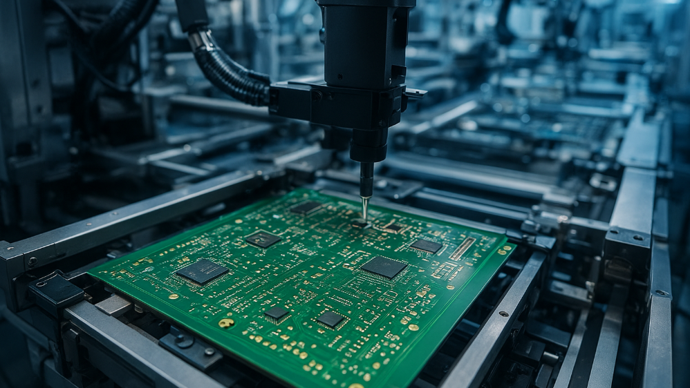
<img src="https://www.gopcba.com/wp-content/uploads/2024/09/BO7B6934.jpg" alt="Spray etching chamber processing a PCB panel on a conveyor” />
Spray Equipment, Conveyors and Regeneration
Production etchers spray the etchant onto both sides of the panel as it travels along a conveyor. Spray pressure, nozzle pattern, oscillation and conveyor speed together determine how evenly the copper is attacked. Uneven spray shows up as a width gradient across the panel, which is why the panel should be centred and why nozzles need checking rather than assuming they are clear.
Regeneration keeps the chemistry in its useful range. In a cupric chloride line the etchant is oxidised back to the active state and the copper is removed by electrolysis or by crystallisation; in an alkaline line the ammonia and the specific gravity are measured and replenished automatically. Without control of these parameters, the etch rate drifts through the shift and so does the finished line width.
Etch Factor, Undercut and Sidewall Shape
The etch factor is the ratio of the depth of copper removed to the amount of lateral undercut, and it is the single number that characterises a process. A high etch factor means straight sidewalls and accurate line width; a low etch factor means the resist edge is undermined and the trace comes out narrower than drawn, with a trapezoidal cross section.
Thin resist, long etch times and aggressive chemistry all reduce the etch factor. Fine line designs therefore need thinner copper and a process that removes the unwanted material quickly, which is why heavy copper and fine pitch rarely go together. Designers should treat the expected undercut as part of the tolerance budget rather than as a manufacturing surprise.
Defects That Come From the Etch Line
The classic etch defect is a sliver, a thin ribbon of copper left between two features that should be isolated. Slivers usually mean the etchant never reached the gap properly, which points at resist that was too thick, a gap that was too narrow, or spray that was blocked. They are dangerous because they can survive visual inspection and only appear as a short at electrical test.
The opposite defect is over etching, which thins traces below specification and can break fine lines entirely. Our notes on copper plating defects and prevention cover the plating side of the same story, and the two processes are usually reviewed together because a plating problem often becomes visible only after etching.
Waste Treatment and Environmental Control
Spent etchant is a hazardous waste stream containing dissolved copper, and it has to be treated rather than discharged. Copper recovery by electrolysis or by precipitation is common, and the rinse water from the etch line must be treated before it leaves the site. These requirements are not optional, and they are part of why etching is normally done in a dedicated facility rather than in a general workshop.
Environmental control in the wider plant matters as much as the chemistry. Our overview of manufacturing environmental controls describes the ventilation, effluent and handling requirements that surround a wet process line, and how those requirements affect what a fabricator can accept.
Tolerances, Design Rules and Fabrication Notes
Because etching removes copper sideways, the finished trace width differs from the drawn width. A fabricator compensates by adjusting the artwork during CAM, usually after measuring the process capability on a test coupon. Designers should therefore supply the nominal widths the circuit needs and state the tolerance, rather than pre-compensating by hand and losing control of the intent.
Where a trace carries significant current, remember that the finished cross section is smaller than the drawn geometry suggests. Our guide to trace width and current calculation explains how to size conductors, and the sizing should include the tolerance that etching introduces.
Inner and Outer Layer Differences
Inner layers are etched before lamination on a thin copper foil, with the resist pattern defining the conductors. Because the copper is thin and the features are later surrounded by resin, the tolerance is usually tighter and the etch factor easier to control. Any defect on an inner layer is buried permanently, which is why inner layer inspection happens immediately after etching rather than at the end of the build.
Outer layers are etched after the plating step, so the copper is thicker and the resist is often the same tin or tin-lead layer that served as the plating mask. PCB etching on outer layers is therefore a double duty operation, and the resist has to survive both the plating bath and the etchant. Where the copper is heavy, the fabricator may etch in two passes or use a different chemistry to reach the required definition without excessive undercut.
FAQ
Why is fine line etching harder than coarse line etching? Because the etchant must penetrate a narrower gap while still removing the copper at a useful rate, and the sidewalls are attacked for longer. Thin copper and thin resist help, which is why fine line processes use thinner foil rather than trying to etch heavy copper more slowly.
Does the etch factor matter for the designer? Indirectly. It sets the achievable tolerance on trace width and spacing, and therefore the smallest features a fabricator can quote. Asking for the fabricator’s minimum width and spacing, rather than assuming a rule of thumb, is the quickest way to keep a design manufacturable.
Can etching defects be repaired? A short caused by a sliver can sometimes be cleared, and an open caused by over etching can occasionally be bridged, but both repairs affect reliability and neither is acceptable for safety critical work. Prevention through process control is far cheaper than rework, especially on fine pitch designs.