High Frequency PCB in Mobile Devices: Materials and Layout
A modern phone or watch contains more radio frequency circuitry than a laboratory instrument did a generation ago, and almost all of it sits on the main board rather than in a separate module. The consequence is that the high frequency PCB in a mobile device is not a specialty board with a radio on it; it is the whole system, with radios, processors, cameras and power management sharing a substrate the size of a credit card.
What the Mobile Board Must Do
It carries several radios operating simultaneously, a processor running at gigahertz rates, high resolution camera interfaces, display interfaces and a power management system that must be efficient enough to run from a battery. The board must also fit inside a metal or glass enclosure that interacts with the antennas and provides very little room for shielding.
Every one of those subsystems has a frequency range, and several of them overlap with the receive bands. The design problem is therefore not merely to route fast signals but to keep each of them from disturbing the others in a volume where physical separation is almost unavailable.
Materials and Hybrid Stackups
Most mobile boards are built on a low loss or modified epoxy laminate with HDI build-up layers, and the radio frequency sections may use a material with a lower loss tangent where the requirement justifies it. A hybrid stack, with the expensive material confined to the layers that carry the radio frequency traces, keeps the cost manageable while meeting the electrical requirement.

The stackup also has to provide the impedance control that the interfaces need and the reference planes that the many separate supply domains require. A typical board has several thin dielectric layers between signal and reference so that the traces can be narrow, which is what allows the routing density the product demands. The arrangement of layers is discussed in layer stackup for one to eight layers.
Impedance Control in a Small Volume
Impedance control in a mobile board is complicated by the geometry. The traces are narrow, the dielectrics thin, and the routing passes under components, through via transitions and beside shielding cans. Each of those changes the local impedance, and the transitions have to be designed rather than accepted.
The design usually specifies the impedance of each critical net, and the fabricator calculates the geometry from the stackup. Where the stack is fine, the calculation is sensitive to the dielectric thickness and to the copper thickness, and the tolerance should be realistic rather than aspirational. The structures available and their sensitivity are described in microstrip and stripline routing.
Antenna and Module Integration
The antennas are the part of the design most affected by the enclosure. A metal frame, a glass back, a camera module and a battery all sit in the near field, and the tuning of an antenna in a phone is done against the final mechanical assembly rather than against the bare board. Multiple antennas must also coexist, which requires isolation between them and careful placement.
A radio frequency module integrates most of the radio but still requires the board to provide a clean supply, a matching network and a defined ground reference. Where the module is connected to an antenna through a trace on the board, that trace must be impedance controlled and its return path continuous. The design techniques are described in EMI suppression design principles.
Shielding and Isolation
Shield cans are used on a mobile board where a circuit needs to be isolated, and they are placed on a grid of grounded pads so that the can makes contact around its perimeter at a spacing that is small compared with the wavelength. A can with a gap at its edge behaves as a slot antenna, which is often worse than no can at all.
The board also has to provide faraday barriers between the digital and radio frequency sections without cutting the return paths of the signals that cross them. Vias stitched along the boundary create a wall that the ground plane can support, and any trace crossing the boundary must do so on a layer where its reference is continuous through the crossing.
Thermal Limits in a Sealed Enclosure
A phone has no fan and little convection, so heat leaves the board by conduction into the frame and the case. The processor, the power amplifiers and the charging circuitry all produce heat, and the surfaces a user touches have limits that the design must respect. Copper area and thermal vias are the tools the board provides.
The power amplifiers are a particular case, because their efficiency falls as they are driven harder and their dissipation rises exactly when the thermal path is least able to cope. The board layout should give them a direct conduction path into the frame, and the thermal design should be evaluated at the case temperature the product allows rather than at room temperature.
Assembly and Mechanical Constraints
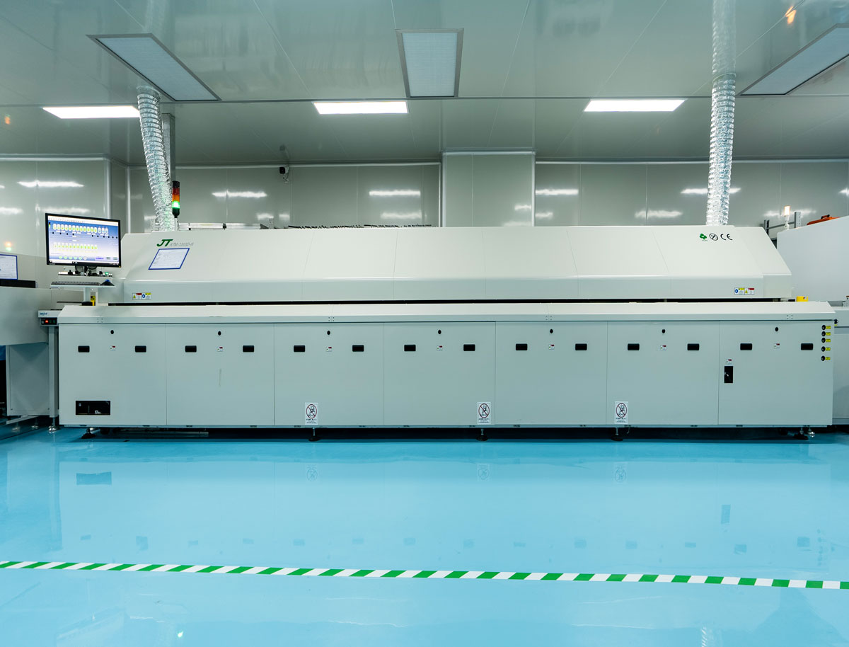
The board is assembled with the most advanced surface mount technology in volume production. Component pitches are at the limit of what placement machines can hold, the stencil is designed for the paste volume that each pad needs, and the reflow profile is chosen for a board whose thickness varies because of the rigid sections and the stiffeners bonded to them.
Mechanically the board is a stressed element. It is screwed or clipped into a frame that flexes slightly when the product is handled, and connectors are loaded every time a cable is inserted. The layout should place the mounting points where they do not load the solder joints of large components, and the ground pads under the shield cans double as mechanical anchors that should be sized for the load rather than for the electrical connection alone.
Test and Yield
Mobile boards are tested at several stages: bare board electrical test on the fine geometry, in circuit test where the design allows it, and functional test of the assembled board. The density makes full probing difficult, so test points are allocated deliberately and the design provides access where a measurement is genuinely needed. A test point that is added without a purpose costs area and adds capacitance to the net it touches, so the test plan should be written together with the layout.
Yield is dominated by the fine pitch devices and the HDI structures. Via in pad with filled and capped microvias, thin dielectrics and small pads all reduce the process window, and the design rules of the chosen fabricator should be the starting point for the layout rather than a constraint discovered later.
FAQ
Does a phone board need a special laminate? The radio frequency sections may, and hybrid stacks are common. The rest of the board uses a low loss or modified epoxy material suitable for HDI processing.
Why do shield cans sometimes make things worse? Because a can that is not bonded around its whole perimeter radiates from the gaps. The stitching pitch and the ground pads under the can are part of the design.
How is the antenna tuned? In the final mechanical assembly, because the frame, battery and camera all shift the resonance. Tuning on the bare board is only a starting point.