Fanout Via Design: Escaping Dense Packages on a PCB
Fanout is the bridge between the package and the board. Before any signal can travel across the board it has to escape the pin field of the device that drives it, and for a large ball grid array that escape is a design problem in its own right. Decisions made during fanout determine how many layers the board needs, how much routing space the rest of the design has, and how the power and ground are distributed.
What Fanout Has to Achieve
A complete fanout gets every signal out of the pin field and into a routing channel, it connects every ground and power ball to the appropriate plane, and it does so without violating the design rules or consuming more board area than necessary. For a large package with hundreds of balls at fine pitch, those requirements compete directly with one another.
The fanout is also where via types are chosen. The choice between a through via, a blind or buried via and a microvia determines how much space each escape consumes and how much the layer stackup has to grow. Because it is decided early, it tends to be inherited by the rest of the design, which is why it deserves deliberate attention rather than being clicked through in an automated routine.
Via Patterns: Dogbone, Via in Pad and Microvia
The traditional pattern places a via beside each pad and connects it with a short trace, forming the shape that gives the dogbone its name. It is simple and cheap, but the trace and the via together occupy more space than the pad alone, which limits how tightly balls can be escaped.
Via in pad places the via directly within the pad, removing the dogbone trace and freeing space between pads. The cost is a more demanding process: the via must be filled and plated over, or tented, to avoid solder wicking during assembly, and that treatment has to be specified. Microvias, formed by laser drilling through a single dielectric layer, allow escapes from fine pitch areas that no through via can reach, at the cost of additional lamination and drilling steps.
<img src="https://www.gopcba.com/wp-content/uploads/2025/08/16-1.png" alt="BGA fanout pattern with dogbone vias on a PCB layout” />
Annular Ring, Drill Size and Layer Count
Every via needs an annular ring, the ring of copper around the hole, and that ring sets the minimum pad diameter. Smaller drills allow smaller pads and denser escapes, but the drill size has an aspect ratio limit determined by the board thickness and the fabricator’s plating capability. A thick board with small holes is a plating problem as much as a routing opportunity.
Layer count follows from the number of escape rows that have to be accommodated. Each routing layer can escape roughly one ring of balls in a given direction, so a package with many rows needs either a stack of layers or a via technology that removes intermediate rows from the through path. Our notes on PCB pad design standards describe the geometry limits that govern the annular ring and pad sizing.
Escape Routing and Channel Assignment
Once signals have left the pin field they have to reach the routing channels, and the direction in which each ring escapes determines how smoothly that happens. Escaping toward the side of the package nearest to the destination reduces congestion, while escaping in a single uniform direction creates a bottleneck at one edge.
Where the package sits in the middle of a board, a radial or quadrant based escape plan usually works better than a directional one, because it spreads the traffic across all four sides. The plan should be drawn before routing starts, since changing it later invalidates every route that depends on it.
Thermal and Assembly Considerations
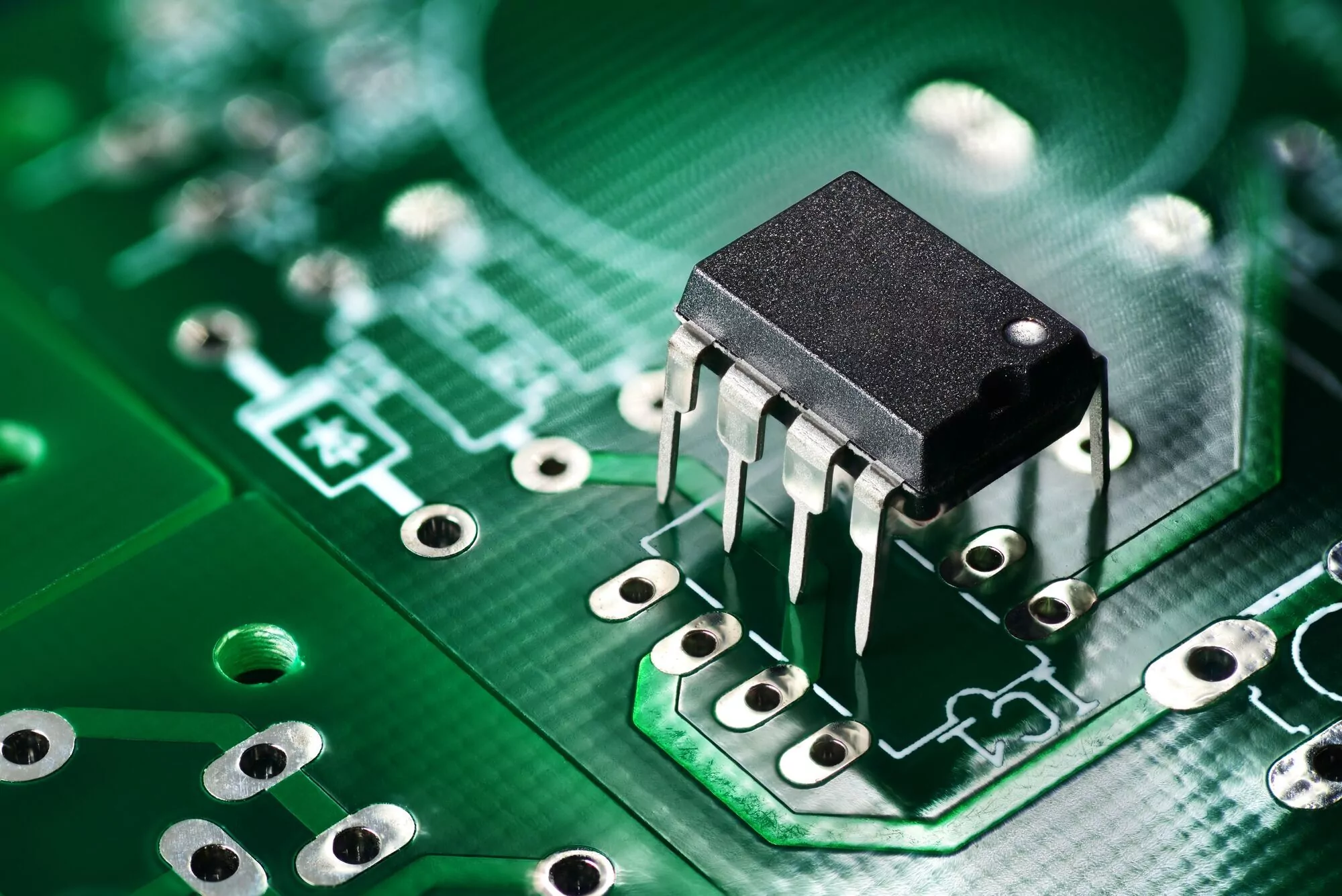
Via in pad is not only a routing technique. A grid of vias under an exposed pad carries heat to the planes below, which is essential for power devices and for packages whose thermal path is through the pad rather than through the leads. The same vias affect the solder joint, because solder can wick through an open hole and starve the joint.
The usual solution is to fill and cap the vias, or to tent them on the opposite side, and to adjust the paste pattern so that the joint forms correctly. Our comparison of thermal via and filled via construction explains when each approach is worth the additional process step.
Designing the Fanout Before Routing
Fanout is a planning activity. The number of escape rows, the via type for each area and the assignment of signals to layers should be decided on paper, with the stackup in front of you, before any routing begins. Doing it in the tool without a plan usually produces a fanout that consumes more layers than necessary and leaves the routing channels fragmented.
The plan also has to respect the electrical requirements. Fast differential pairs that have to stay on one layer for impedance reasons may not tolerate the two vias that a dogbone fanout would add, and power balls that carry high current need enough vias to keep the resistance and inductance low. Our notes on high speed PCB layout floorplanning describe how those constraints are combined with the mechanical ones.
Common Fanout Mistakes
The most frequent mistakes are familiar. Using through vias everywhere on a fine pitch package and then discovering that the resulting stackup is two layers thicker than the project can afford. Escaping all signals in one direction and creating congestion at one edge. Forgetting the ground balls, or connecting them with a single thin trace instead of a via per ball. Leaving the thermal pad without a via array and relying on the leads for heat transfer.
A design review that looks at the fanout plan rather than at the finished routing catches all of these while they are still cheap to correct, which is the strongest argument for treating fanout as a design decision rather than a tool operation.
Documenting the Fanout for Assembly
The fanout also has to be documented for the people who will build the board. If via in pad is used, the fabrication drawing must say so and specify the fill and cap requirement; if microvias are used, the stackup has to show which layers they connect and how many sequential lamination cycles are implied. An assembler who does not know that vias sit inside the pads will use a standard paste pattern and discover the problem only when the joints come out starved.
FAQ
When should I use via in pad? When the escape density demands it or when the thermal path requires it, and when the assembly process can support filled and capped vias. On a coarse package with plenty of space, a dogbone fanout is simpler and cheaper and creates fewer process risks.
How many vias does a ground ball need? At least one, placed as close to the ball as the geometry allows, and more where the ball carries significant current or where the return path matters for signal integrity. Connecting several ground balls with a chain of traces is a poor substitute for individual vias.
Can I change the fanout after routing? Technically yes, practically it is expensive. The fanout determines the layer assignment that everything else depends on, so a change usually invalidates a large part of the routing and can force a stackup revision. Plan it first.