
Microvia Reliability in HDI Board Design and Assembly
Microvias are the small laser-drilled holes that let HDI boards pack more routing into less space, and they are also the feature most likely to fail a thermal cycling test. Because the hole is only a fraction of a millimetre deep and plated through a thin dielectric, microvia reliability depends on a chain of decisions that starts in the stackup and ends on the assembly line. This guide covers the geometry, plating, and material factors that keep those interconnects intact.
Why Microvia Reliability Drives HDI Yield
A microvia is typically 50 to 150 micrometres in diameter and connects one build-up layer to the next through a dielectric that may be thinner than 60 micrometres. That short barrel is mechanically weaker than a conventional plated through hole, and it sits directly above a copper target pad that acts as a stress riser. When the barrel cracks, the failure often appears as an intermittent open rather than a clean break.
Reliability therefore has to be designed and then verified, not inspected in. A build that passes electrical test at the fabricator can still open after three reflow passes or a hundred thermal cycles if the plating is thin at the target interface. Understanding the failure mechanisms lets you set plating targets, coupon tests, and design rules that reflect how the product will actually be used.
Microvia Geometry: Diameter, Depth and Aspect Ratio
The aspect ratio of a microvia is its depth divided by its diameter, and it is the single most useful predictor of plating quality. A shallow, wide via fills with copper easily, while a deep, narrow one starves the middle of the barrel and thins near the bottom corner. Most fabricators publish a working limit, commonly around 0.75 to 1.0 for laser-drilled microvias in standard build-up dielectrics.
Depth is set by the dielectric thickness, which in turn follows the resin content and the lamination cycle. Squeezing the dielectric thinner improves the aspect ratio but reduces the insulation margin and can cause the laser to strike the layer below. Diameter is limited by drill resolution and registration tolerance. The usable window comes from balancing all three rather than optimising one.
Copper Plating Uniformity Inside Tiny Holes
Electroplating depends on electrolyte exchange, and a microvia has very little room for it. Additives in the bath, current density, and agitation all determine whether the copper builds evenly from the surface to the bottom corner. Problems show up as thin plating at the target pad, a void where the barrel meets the pad, or a barrel that separates when the board is stressed by press-fit connectors or thermal load.
Fabricators manage this with periodic microsections of test coupons, plating thickness measurements on the surface and inside the barrel, and bath analysis by titration or cyclic voltammetry. As a buyer, you should ask which coupon and which locations are used, and whether surface copper thickness is reported separately from hole wall deposits. The two are not interchangeable, and conflating them hides weak interconnects.
Stacked, Staggered and Skip Via Structures
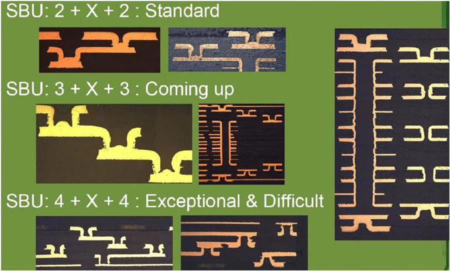
Stacked microvias place one via directly on top of another, forming a vertical tower through several layers. They save routing area and shorten the path, but each interface concentrates stress, and a weak plating seam at any level can propagate. Staggered microvias offset each layer, spreading the load and generally offering better fatigue life at the cost of more routing space.
Skip vias reach across more than one layer in a single lamination cycle, reducing the number of sequential builds. They demand better drill depth control and dielectric uniformity because the hole is deeper. Whichever structure you choose, the stackup drawing, the drill table, and the fabrication notes must describe the same thing, since fabricators work from the stackup and will not infer intent.
Dielectric Materials and CTE Mismatch
Each reflow or thermal excursion expands the resin and the copper by different amounts. The dielectric expands far more along the z axis than the copper does, so the barrel is stretched while the pad beneath it is not. A high coefficient of thermal expansion, a low glass transition temperature, or a resin that softens early all make that mismatch worse and shorten the time to a crack.
Material selection is therefore part of the reliability budget. Filled resins with lower expansion, higher glass transition temperatures, and better dimensional stability reduce the strain on every microvia in the build. The trade-off is cost, drill difficulty, and sometimes electrical performance. Matching the laminate to the expected thermal environment is cheaper than adding layers to compensate for weak interconnects later.
Thermal Cycling and Interconnect Stress Testing
Because field failures take years to appear, the industry accelerates them. Interconnect stress testing passes a controlled current through a daisy-chained coupon, heating it to a set temperature, then cools it while monitoring resistance. A rise beyond a small threshold signals that a barrel has cracked. Thermal cycling between fixed extremes, and reflow simulation, work on the same principle with different stress profiles.
Coupon design matters as much as the test. The chain must include the smallest vias in the build, the highest aspect ratio, and the layers that see the most sequential lamination. Test results should be recorded per lot and trended, so that a drift in plating or lamination is caught before it reaches production panels. A single passing coupon proves far less than a chart of consistent ones.
Via Filling and Capping Options
Many HDI designs require a flat surface above a microvia, especially under fine-pitch BGA pads. Conductive or non-conductive via filling paste is pressed into the hole, cured, and then planarised, after which copper plating and capping create a solid pad. Done well, this removes the cavity that traps flux and eliminates the void that would otherwise form under the ball.
Filling is not trivial on small holes. Incomplete fill, trapped solvent, or shrinkage during cure creates voids that appear later as blowholes or as measling in the laminate. The process window is narrow, so paste properties, print parameters, and cure profile need to be qualified together. Ask for cross-sections of filled vias, not just a statement that the step is offered.
Assembly Stress: Reflow, Rework and Handling
Assembly exposes microvias to their harshest short-term conditions. Multiple reflow passes, a localised rework cycle with hot air, and mechanical handling all add strain. Rework is especially risky because the board is heated locally while the rest of the panel stays cool, producing a steep thermal gradient across the build-up layers. Repeated rework at the same site compounds the damage.
Good practice limits the number of rework cycles, preheats the assembly before local heating, and records which boards received rework so that reliability assumptions stay honest. For area-array packages, a proper reball and replacement procedure keeps the thermal load predictable rather than improvised. Handling also matters: flexing a thin HDI board during depanelisation can crack a microvia that no electrical test will catch.
Design Rules and Process Control That Protect Yield
Start with the stackup and confirm that no dielectric is asked to do more than the fabricator can plate reliably. Keep the capture pad large enough to tolerate registration error, avoid placing a microvia directly on a pad edge, and stagger rather than stack unless the routing gain justifies the risk. Where a stack is unavoidable, reduce the number of sequential steps and use materials with lower expansion.
On the process side, control laser energy, desmear, and plating chemistry as one system. Microsections, plating thickness data, and interconnect stress test results should be reviewed together, because a change in any one of them usually shows up in the others first. Document the limits in the fabrication drawing and review them whenever the supplier, laminate, or build-up changes.
FAQ
What aspect ratio is safe for a microvia? Most fabricators work comfortably up to about 0.75 to 1.0 for laser-drilled microvias in standard build-up dielectrics, and some can go higher with specialised chemistry. The safe value depends on your plating line and the dielectric, so ask for microsection evidence at the ratio you intend to use rather than relying on a general figure.
Are stacked microvias less reliable than staggered ones? Generally yes, because every interface between two barrels concentrates stress and any weak seam can propagate upward. Stacked structures remain useful where routing density demands them, but they deserve lower-expansion materials, tighter plating control, and qualification by thermal cycling rather than by electrical test alone.
How do I verify microvia plating thickness? Request microsections through the smallest vias in the build, with measurements taken at the surface, mid-barrel and the target pad corner. Pair those results with interconnect stress test data from a coupon that includes the same geometry. Surface copper readings alone cannot confirm that the barrel is adequately plated.